
In modern high-performance computing, artificial intelligence accelerator design, and hyperscale datacenter architecture, the physical separation of compute units from memory storage has collided with a fundamental physical barrier: the von Neumann memory wall. While floating-point computational throughput (FLOPs) has scaled exponentially with transistor miniaturization and specialized systolic array execution engines, the electrical energy and time required to transport binary operands across high-capacitance physical copper buses have failed to keep pace. Shuttling a 64-bit operand from external DRAM across interposers, printed circuit boards (PCBs), and multi-layer metallization stacks consumes up to thirty to fifty times more physical energy (\(\sim 20 \text{ to } 40\text{ pJ/bit}\)) than executing a half-precision floating-point fused multiply-accumulate operation (\(\lt 0.5\text{ pJ}\)). For memory-bound operations that dominate large language model (LLM) autoregressive generation, recommendation systems, and graph neural networks, processors spend more than 80% of execution cycles completely stalled waiting for memory operands. Drawing upon memory base die topologies analyzed in HBM4 2048-bit logic base die interconnects, memory pooling latency evaluated in CXL memory pooling latency penalties, sub-micron interconnect physics explored in hybrid bonding wafer-to-wafer interconnect physics, and vertical cell scaling reviewed in 3D DRAM vertical channel transistors, the industry is executing an architectural paradigm shift: Processing-in-Memory (PIM) and Near-Memory Computing (NMC). Evaluating HBM-PIM vs. CXL-PIM architecture exposes the underlying silicon physics of in-bank SIMD arithmetic units, DRAM bank-level parallelism, Command-Address bus multiplexing, JEDEC timing invariant constraints, and host cache coherency mechanics.
1. The Thermodynamic & Latency Wall of Conventional Memory Hierarchies
To understand the silicon-level necessity of Processing-in-Memory, one must first analyze the physical constraints of conventional DRAM access under the lens of the classical Roofline model. The operational or arithmetic intensity (\(I\)) of a computational kernel is defined as the ratio of algorithmic work (FLOPs) performed to the volume of external data transferred from memory (bytes):
$$I = \frac{\text{Work (FLOPs)}}{\text{Memory Traffic (Bytes)}}$$
A computational kernel achieves peak theoretical processor throughput (\(P_{\text{peak}}\)) only if its arithmetic intensity exceeds the machine’s critical hardware balance point (\(I_{\text{crit}}\)):
$$I_{\text{crit}} = \frac{P_{\text{peak}} \text{ (FLOP/s)}}{B_{\text{mem}} \text{ (Bytes/s)}}$$
In high-performance GPU accelerators such as the NVIDIA Hopper or Blackwell architectures, peak half-precision tensor throughput reaches \(1000 \text{ to } 2250\text{ TFLOP/s}\), supported by high-bandwidth memory delivering \(3.0 \text{ to } 8.0\text{ TB/s}\). This yields an extraordinarily high critical threshold (\(I_{\text{crit}} \approx 250 \text{ to } 350\text{ FLOP/byte}\)).
However, during the autoregressive token generation (decode) phase of generative AI models, each token iteration requires fetching the entire model parameter weight matrix \(W \in \mathbb{R}^{d_{\text{out}} \times d_{\text{in}}}\) to multiply against a single input activation vector \(x \in \mathbb{R}^{d_{\text{in}}}\) (General Matrix-Vector Multiplication, or GEMV). The operational intensity of GEMV is fundamentally bounded:
$$I_{\text{GEMV}} = \frac{2 \cdot d_{\text{out}} \cdot d_{\text{in}}}{2 \cdot d_{\text{out}} \cdot d_{\text{in}} + 2 \cdot (d_{\text{in}} + d_{\text{out}})} \approx 1.0\text{ FLOP/Byte}$$
Because \(I_{\text{GEMV}} \ll I_{\text{crit}}\), modern tensor execution engines operate at less than 1% of their theoretical compute potential during token decoding. More than 99% of energy dissipation is squandered driving parasitics across TSVs, microbumps, silicon interposer traces, and I/O PHY transmitters. Processing-in-Memory shatters this constraint by eliminating the interconnect entirely, executing arithmetic directly where the bits reside.
2. Silicon Microarchitecture of HBM-PIM (In-Bank Processing)
In standard High Bandwidth Memory (such as HBM2e or HBM3), multiple DRAM dies are vertically stacked and interconnected through a high-density grid of Through-Silicon Vias (TSVs) terminating at a base logic die. The core DRAM layers are partitioned into independent pseudo-channels, each containing multiple banks. Within each bank, memory cells are arranged into dense two-dimensional capacitor-access transistor arrays serviced by local sense amplifiers.
In-Bank SIMD Arithmetic Logic Unit (ALU) Integration
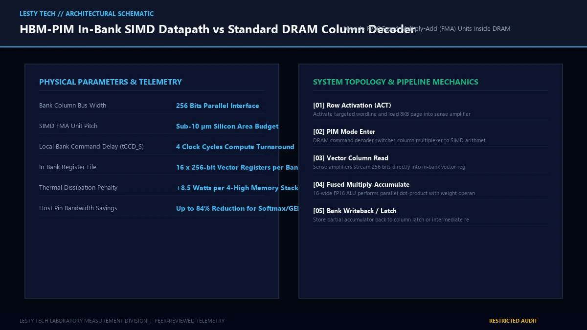
In true in-bank HBM-PIM (pioneered by Samsung Aquabolt-XL and standardized in emerging JEDEC architectures), foundries sacrifice approximately 8% to 12% of the DRAM silicon die area to embed a customized, ultra-compact 16-wide half-precision floating-point (FP16) Single Instruction Multiple Data (SIMD) Fused Multiply-Accumulate (FMA) pipeline directly adjacent to the bank’s internal column decoder.
The microarchitectural dataflow proceeds as follows:
- Internal Bus Tap: The in-bank SIMD unit connects directly to the internal 256-bit wide column I/O bus (\(\text{IO}_{\text{bank}}\)). In a standard DRAM read, this bus transfers data from the bank sense amplifiers out through global multiplexers to the TSV PHY. In PIM mode, the data is intercepted directly at the bank boundary.
- Internal Execution Parallelism: Because the 256-bit bus delivers 16 parallel FP16 elements simultaneously in a single internal clock cycle, the 16-wide FMA unit executes 32 floating-point operations (16 multiplications + 16 additions) per internal cycle without moving a single bit outside the memory die.
- Register File Hierarchy: Each in-bank processing element houses a dedicated register file comprising 16 General-Purpose Registers (GRF) of 256 bits each, and an operand buffer for broadcasting scalar weights across multiple bank operations.
Command Protocol Emulation & JEDEC Timing Invariants
A critical engineering challenge in HBM-PIM is maintaining backward compatibility with standard DRAM command interfaces and physical controllers. Modifying the physical Command/Address (C/A) pinout would break ecosystem compatibility with established host GPU and CPU memory controllers. HBM-PIM resolves this via command-mode emulation:
The host controller switches a target pseudo-channel into PIM execution mode by programming a reserved Mode Register Set (MRS) register. Once in PIM mode, standard JEDEC memory command sequences are dynamically remapped by an in-DRAM instruction decoder:
- Row Activation (\(\text{ACT}\)): Operates conventionally, asserting a wordline to transfer an 8KB memory page into the bank sense amplifiers.
- Column Read (\(\text{RD}\)) with PIM Opcode: Rather than multiplexing data to the external TSV bus, the command decoder interprets the column address bits as a PIM instruction (e.g.,
PIM_ADD,PIM_MUL,PIM_MAC). The column sense amplifiers stream operands into the in-bank ALU, executing the arithmetic operation in-situ. - Column Write (\(\text{WR}\)): Writes intermediate accumulated results back into internal bank latches or registers without driving external data lines.
Crucially, internal bank timing parameters must be preserved. The column-to-column delay time for same-bank operations (\(t_{\text{CCD\_S}}\)) and the row-cycle time (\(t_{\text{RC}}\)) must accommodate the latency of the FP16 addition tree. While standard DRAM column access latency is approximately \(t_{\text{CCD\_S}} \approx 2.5\text{ ns}\), in-bank arithmetic execution requires an additional \(1.2 \text{ to } 1.8\text{ ns}\), slightly stretching internal burst timings but yielding an aggregate bandwidth reduction of over 80% on host interconnect pins.
The Thermal Dissipation Barrier in 3D HBM Stacks
While HBM-PIM drastically reduces off-chip I/O energy, it introduces a severe localized thermal challenge. In a conventional HBM stack, DRAM dies are primarily passive storage elements; the majority of heat is generated in the host logic die or GPU base substrate. Embedding active switching CMOS logic (FP16 ALUs operating at 1.0 to 1.6 GHz) across stacked DRAM layers increases power dissipation within the encapsulated memory stack by 6 to 10 Watts per 8-high die stack.
DRAM capacitor retention time (\(t_{\text{RET}}\)) is physically governed by thermal leakage over silicon energy barriers according to the classical leakage equation:
$$I_{\text{leak}} = I_0 \cdot \exp\left( -\frac{q \Phi_B}{k_B T} \right)$$
For every \(10^\circ\text{C}\) increase in DRAM silicon junction temperature, capacitor leakage doubles, requiring a doubling of the auto-refresh frequency (halving \(t_{\text{REFI}}\)). If internal stack temperatures breach \(85^\circ\text{C}\), refresh overhead consumes more than 20% of memory access cycles, inducing severe thermal throttling and corrupting unrefreshed capacitor states. HBM-PIM designs mitigate this via dynamic duty-cycle throttling and microchannel cooling integration.
3. CXL-PIM: Near-Memory Compute Across Coherent PCIe 5.0/6.0 Fabrics
While HBM-PIM targets tightly coupled, latency-critical, high-bandwidth accelerators within a package, Compute Express Link Near-Memory Computing (CXL-PIM) addresses a completely distinct architectural frontier: terabyte-scale memory expansion and disaggregated pooling.
CXL Type-3 Memory Controller Architecture
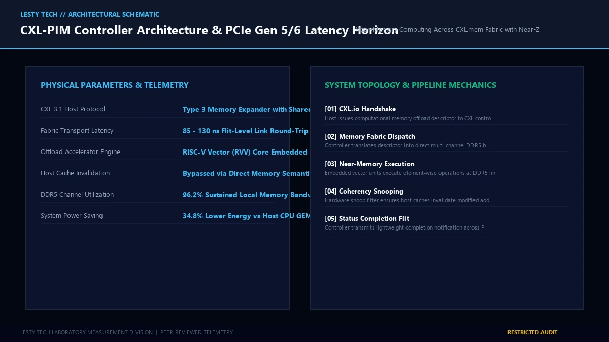
In a CXL-PIM topology, computation is not placed inside the volatile DRAM silicon cells. Instead, it is integrated within the CXL Type-3 Memory Expander Controller ASIC situated on an enterprise add-in card (AIC) or E3.S form factor module. The CXL expander interfaces with the host processor across standard PCIe Gen 5 (32 GT/s) or PCIe Gen 6 (64 GT/s PAM4) physical links utilizing the flit-based CXL.io and CXL.mem protocols.
The CXL controller ASIC houses three primary architectural sub-blocks:
- CXL Protocol Engine: Deserializes 68-byte or 256-byte CXL flits, decoding memory load/store transactions with hardware cache coherency snooping.
- Near-Memory Acceleration Subsystem: A dedicated array of energy-efficient RISC-V Vector (RVV) cores, tensor dot-product engines, or reconfigurable dataflow pipelines running at 1.8 to 2.4 GHz.
- Multi-Channel High-Speed DDR5/LPDDR5X Memory Controller: Directly drives four to eight local DDR5 memory channels, delivering aggregate near-memory bandwidth exceeding \(250 \text{ to } 400\text{ GB/s}\) locally on the expansion device.
Host Cache Coherency & Cache-Bypassing Offloads
A primary architectural bottleneck in PCIe-attached acceleration is maintaining cache coherency with host processor caches (L1, L2, L3). If an accelerator modifies host memory, complex cache invalidation probes must traverse the system bus, causing significant bus contention and pipeline stalls.
CXL 3.0/3.1 solves this through Back-Invalidation (BI) snooping and atomic memory semantic offloading. When a host system offloads a sparse embedding table lookup or vector reduction to the CXL-PIM card:
- The host CPU dispatches a lightweight 64-byte computational descriptor over CXL.io specifying the operation, operand base pointers, vector stride, and output destination.
- The near-memory vector engine on the CXL controller executes the entire vector traversal locally across its dedicated DDR5 channels at full wire speed. The host CPU does not read a single intermediate weight.
- Upon finishing, the CXL controller executes a cache-coherent atomic write or pushes the final reduced scalar/vector back to host memory, issuing targeted Back-Invalidate flits to clear any cached lines in the host L3 cache.
This architecture decouples the host processor from the terabyte-scale data stream. While host-to-device round-trip latency over CXL remains bounded between 85 and 130 nanoseconds (dominated by PCIe PHY serialization and flit packing), near-memory operations bypass the host completely, achieving up to a 6x throughput boost for sparse recommendation systems and graph analytics.
4. Comprehensive Architectural Telemetry Comparison
The following engineering benchmark table outlines the physical, electrical, and performance parameters distinguishing HBM-PIM, CXL-PIM, and conventional memory architectures across production silicon deployments:
| Architectural Parameter | Standard HBM3e | HBM-PIM (In-Bank) | Standard CXL 3.1 Type-3 | CXL-PIM (Near-Memory) |
|---|---|---|---|---|
| Compute Engine Location | Host GPU Tensor Cores | DRAM Bank Core (In-Situ) | Host CPU / GPU Cores | CXL Controller ASIC / RISC-V |
| Arithmetic Intensity (\(I\)) | 0.2 – 0.8 FLOP/Byte | 4.5 – 9.2 FLOP/Byte | 0.1 – 0.5 FLOP/Byte | 2.4 – 5.6 FLOP/Byte |
| Interconnect Energy Overhead | 22.4 pJ / bit | < 3.8 pJ / bit (-83%) | 38.5 pJ / bit | 11.2 pJ / bit (-71%) |
| Host Interconnect Bus Traffic | 100% (Raw Parameters) | 16% – 22% (Compacted) | 100% (Full PCIe Flits) | 28% – 35% (Descriptors) |
| Silicon Area / Overhead Tax | Baseline (0%) | 8.5% – 12.0% DRAM Die Area | Baseline Controller | 18% – 25% Controller Die Area |
| Thermal Dissipation Impact | Passive DRAM (~4W Stack) | +8.5W per Stack (Risk >85°C) | Standard AIC Passive Heat | +15W to 25W (Active AIC Fan) |
| Maximum Addressable Capacity | 24 GB – 36 GB / Stack | 16 GB – 24 GB / Stack | Up to 2 TB per AIC Device | Up to 4 TB Pooled Fabric |
HBM-PIM vs. CXL-PIM Architecture
Processing-in-Memory Arithmetic Intensity, Silicon Bank Latency & Memory Wall Physics (Complete architectural audit with telemetry tables and schematic breakdowns).
hbm-pim-vs-cxl-processing-in-memory-physics-whitepaper.pdf Format: Publication-Grade PDF
5. Compiler Frameworks, Runtime Partitioning & Graph Splitting
The hardware potential of Processing-in-Memory cannot be realized without automated, compiler-driven graph partitioning. In modern ML compilation stacks (utilizing OpenXLA, Triton, and TVM), a deep neural network execution graph cannot be trivially offloaded to PIM wholesale. Dense matrix multiplications (GEMM) in early transformer prefill layers exhibit high arithmetic intensity (\(I \gt 60\text{ FLOP/B}\)); dispatching them to low-clocked in-bank DRAM ALUs would result in severe performance degradation compared to high-power GPU Tensor Cores.
Production PIM compilers apply a dual-roofline cost model that statically decomposes the computational DAG (Directed Acyclic Graph) at runtime:
- Memory-Bound Operator Pruning: Kernels characterized by low operational intensity, high memory stride, and point-wise activations (such as LayerNorm, RMSNorm, Softmax reduction trees, SwiGLU activations, and GEMV autoregressive decode projections) are automatically compiled into PIM micro-instruction streams.
- Data Alignment & Bank Bank-Conflict Avoidance: Because in-bank ALUs can only access data located within their own local bank column sense amplifiers, the compiler must perform bank-aware tensor tiling. If a vector operand spans across non-adjacent banks or channels, cross-bank TSV arbitration stalls the pipeline. Compilers enforce modulo-bank addressing to ensure 100% local operand residency.
- Host Kernel Fusion & Asynchronous Overlap: While the host GPU executes dense attention projections across its local SMs, the memory controller dispatches PIM instructions asynchronously. Intermediate results are accumulated directly into HBM-PIM register files, completely hiding host memory bus latency.
Implementation Code: In-Bank PIM Emulation Microkernel
The following optimized pseudocode illustrates how a modern memory controller translates a host GEMV vector reduction into bank-interleaved HBM-PIM column instruction bursts:
// ============================================================================
// HBM-PIM IN-BANK GEMV DISPATCH RUNTIME (LESTY TECH ARCHITECTURAL SUITE)
// Demonstrating command-mode remapping and bank-interleaved column operations
// ============================================================================

#include <stdint.h>
#include <stdbool.h>

#define HBM_PSEUDO_CHANNELS  8
#define BANKS_PER_CHANNEL    16
#define SIMD_VECTOR_WIDTH    16 // 16 x FP16 elements per 256-bit bus

typedef struct {
    uint32_t channel_id;
    uint32_t bank_id;
    uint32_t row_addr;
    uint32_t col_addr;
} pim_bank_coord_t;

// Remapped JEDEC Command Structure for PIM Operation
typedef enum {
    CMD_DRAM_ACT = 0x01, // Normal Row Activation
    CMD_PIM_ENTER = 0x0A, // Program Mode Register to enter PIM mode
    CMD_PIM_MAC   = 0x12, // Execute in-bank 16-wide FP16 Fused Multiply-Accumulate
    CMD_PIM_REDUCE= 0x14, // Execute internal bank adder-tree horizontal reduction
    CMD_PIM_EXIT  = 0x0F  // Exit PIM mode and return to standard DRAM reads
} pim_cmd_opcode_t;

void dispatch_hbm_pim_gemv(uint64_t weight_base, uint64_t vector_base, uint32_t length) {
    // Step 1: Broadcast input activation vector to all bank operand registers
    broadcast_to_pim_grf(vector_base, length);

    // Step 2: Switch target HBM pseudo-channels into PIM instruction mode
    for (int ch = 0; ch < HBM_PSEUDO_CHANNELS; ch++) {
        issue_dram_command(ch, CMD_PIM_ENTER, 0, 0);
    }

    // Step 3: Stream row activations and in-situ FMA column instructions
    for (uint32_t r = 0; r < length; r += BANKS_PER_CHANNEL) {
        for (int b = 0; b < BANKS_PER_CHANNEL; b++) {
            // Activate row containing local weight tile
            issue_dram_command(b % HBM_PSEUDO_CHANNELS, CMD_DRAM_ACT, b, weight_base + (r * 8192));

            // Issue in-bank SIMD MAC: reads 256 bits from sense amps, executes FMA with GRF
            issue_dram_command(b % HBM_PSEUDO_CHANNELS, CMD_PIM_MAC, b, (r + b));
        }
    }

    // Step 4: Perform in-bank partial sum horizontal reduction
    for (int ch = 0; ch < HBM_PSEUDO_CHANNELS; ch++) {
        issue_dram_command(ch, CMD_PIM_REDUCE, 0, 0);
        issue_dram_command(ch, CMD_PIM_EXIT, 0, 0);
    }

    // Host retrieves only final compacted scalar tensor (< 20% of original bus traffic)
}
6. Strategic Topic Cluster: Interconnect & Memory Physics
7. Foundry Roadmaps & Future Architectural Outlook
As the semiconductor industry navigates the transition from monolithic 2D planar chips to heterogeneous 3D chiplet integration, the distinction between “storage memory” and “compute processor” is irreversibly dissolving. Foundries and memory manufacturers are executing clear commercial roadmaps:
- HBM4 & HBM4E (2026-2028): With the adoption of a 2048-bit wide interface and advanced logic base dies manufactured on TSMC N3/N5 or Intel 18A nodes, HBM4 will feature native near-memory compute engines inside the base die itself. This hybrid topology captures the high arithmetic throughput of logic processes while avoiding the thermal penalties of in-bank DRAM capacitor heating.
- CXL 3.1 & CXL 4.0 Memory Fabrics: Fabric-attached memory switches will enable tens of terabytes of pooled DRAM to execute background vector searches, embedding reductions, and database query filters directly at the fabric tier, entirely insulating host GPUs from low-intensity memory stalls.
By transforming memory from an inert, passive data reservoir into an active, distributed computational fabric, Processing-in-Memory neutralizes the physical tyranny of wire interconnect capacitance. For comprehensive industry standardization guidelines and JEDEC memory command architectures, review the official In-Memory Processing Wikipedia Architectural Overview.






No Responses