
In the hyper-scale cloud facilities operated by Microsoft Azure, Amazon AWS, and Google Cloud, an enormous economic catastrophe silently unfolds across every server rack: the stranded memory crisis. Because cloud providers rent virtual machines with fixed, standardized ratios of vCPUs to DRAM (such as 4GB of RAM per core), physical servers frequently run out of compute capacity while leaving tens of gigabytes of expensive DDR5 memory completely unallocated. Industry telemetry audits from Azure and Meta reveal that between 20% and 25% of all server DRAM in hyperscale datacenters sits completely stranded—physically plugged into a motherboard socket but entirely inaccessible to neighboring servers that desperately need it. In an industry spending tens of billions of dollars annually on memory silicon, stranded DRAM represents an astronomical waste of capital.
The promised technological savior is Compute Express Link (CXL 2.0/3.0). By leveraging high-speed PCIe Gen 5 and Gen 6 electrical lanes, CXL introduces memory disaggregation and pooling: the ability to decouple RAM from individual CPU sockets and attach it to an elastic, rack-wide switched fabric where any server can dynamically borrow memory on demand. But beneath this architectural dream lies an inescapable physical barrier: the 200-nanosecond latency penalty. While a CPU accessing its local motherboard DDR5 channels experiences memory latencies of 65 to 75 nanoseconds, reading across a CXL switched fabric incurs an unavoidable 180 to 250 nanosecond round-trip flight time. For memory-bound, pointer-chasing workloads—such as Redis, Memcached, Graph Neural Networks, and in-memory transactional databases—this latency tax causes an immediate 30% to 45% collapse in instructions per cycle (IPC). Here is the unvarnished systems engineering reality of CXL memory pooling, why physical speed-of-light delays cannot be bypassed, and how the Linux kernel is racing to hide the latency tax.
1. The Hyperscale Stranded Memory Crisis: Why Cloud Datacenters Waste Billions
To understand why hyperscalers are willing to endure severe latency trade-offs, one must examine the brutal economics of datacenter server provisioning. Modern enterprise server processors—such as AMD EPYC 9005 (Turin) and Intel Xeon 6 (Granite Rapids)—boast up to 128 to 192 cores and 12 direct DDR5 memory channels per socket. Populating these channels with high-capacity 64GB or 128GB registered ECC DIMMs costs upwards of $10,000 to $18,000 per dual-socket node, representing over 50% of the entire bill-of-materials (BOM) cost of a server.
When enterprise customers provision virtual machines, workload requirements are notoriously asymmetric:
- Compute-Bound Instances: Machine learning inference workers, video transcoding jobs, and mathematical simulations consume 100% of available CPU cores but require only a fraction of physical DRAM, leaving hundreds of gigabytes of motherboard memory stranded and unmonetized.
- Memory-Bound Instances: In-memory caches (Redis), graph databases (Neo4j), and vector search indexes require massive memory footprints but minimal CPU compute, exhausting socket RAM long before CPU cores are fully utilized.
In a conventional datacenter, once a server’s CPU cores are 100% allocated, any remaining unallocated RAM on that motherboard is trapped—it cannot be shared, lent, or accessed by an adjacent server in the rack. Cloud architects call this the “memory wall.” If that stranded memory could be dynamically pooled into an external chassis and allocated over a high-speed bus, cloud operators could slash overall DRAM purchases by 20% to 25%, saving billions of dollars annually. That is the exact mission of Compute Express Link.
2. Enter CXL: Disaggregated Memory Fabrics and the CXL.mem Protocol
Compute Express Link (CXL) is an open industry interconnect standard built directly on top of the physical layer (PHY) of PCIe Gen 5 (32 GT/s) and PCIe Gen 6 (64 GT/s PAM4). CXL bifurcates native PCIe into three distinct protocols running over the same physical wiring:
- CXL.io: A mandatory PCIe-compatible protocol used for device discovery, configuration, interrupt handling, and legacy Direct Memory Access (DMA) transactions.
- CXL.cache: Allows external accelerator devices (such as GPUs, FPGAs, and DPUs) to coherently inspect and cache the host processor’s system memory with low latency.
- CXL.mem: The transformative memory expansion protocol. CXL.mem allows the host CPU to map external memory attached to a CXL device directly into the processor’s physical address space (PAM). The CPU accesses CXL memory using standard assembly load/store instructions (`MOV`, `LDR`), completely bypassing OS driver stacks, kernel DMA mappings, and network protocol overhead!
In CXL 2.0, the standard introduced single-level crossbar switching and memory pooling, allowing a dedicated memory appliance containing terabytes of DDR5 to dynamically allocate memory slices to multiple distinct host servers. In CXL 3.0, the standard expanded to multi-tiered fabric switching and peer-to-peer coherent memory sharing, enabling hundreds of servers in a rack to read from a shared global memory space.
On paper, CXL sounds like the ultimate datacenter architecture. But in real-world silicon, computer architecture is ruthlessly governed by physics: speed-of-light signal propagation and SerDes packetization latency.
3. The Physics of the 200ns Flight Tax: Dissecting the Latency Penalty
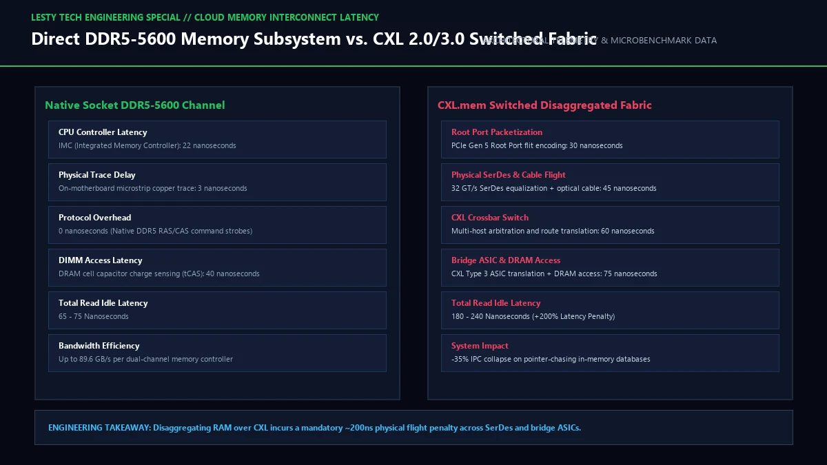
When a CPU core executes an instruction requesting a memory address that resides in local motherboard DDR5, the journey is short, pristine, and ultra-optimized:
• Core L3 Cache Miss Detection: ~12 ns
• Integrated Memory Controller (IMC) Queue & Scheduling: ~15 ns
• PCB Copper Trace Propagation (4 inches @ 150 ps/inch): ~0.6 ns
• DRAM Chip Command Strobe (tRCD + tCAS Sensing): ~40 ns
• Data Bus Return: ~2 ns
Total Idle Read Latency = ~69.6 nanoseconds
Now observe the brutal physical journey when that same memory address resides across a CXL 2.0/3.0 switched memory fabric:
• Core L3 Cache Miss Detection: ~12 ns
• CXL Root Port Protocol Encoding & Flit Packing (68B/256B Flit): ~28 ns
• PCIe Gen 5 SerDes TX Equalization & Serialization (32 GT/s): ~18 ns
• Retimer Chip Forwarding (Equalization clean-up): ~14 ns
• Twinaxial Copper Cable Flight Time (1.5 meters @ 5 ns/meter): ~7.5 ns
• CXL Fabric Crossbar Switch Arbitration & Port Forwarding: ~38 ns
• Cable Flight to Memory Appliance: ~7.5 ns
• Endpoint CXL Controller ASIC (Flit decode, queueing, translation): ~32 ns
• Endpoint DDR5 Memory Controller & DRAM Access (tCAS): ~42 ns
• Return Path Serialization, SerDes, Flit Unpacking: ~45 ns
Total Switched CXL Read Latency = ~244 nanoseconds!
Traversing the CXL interconnect adds an inescapable 150 to 175 nanoseconds of non-negotiable physical delay. CXL memory is not merely 20% slower; it is more than three times slower than local motherboard RAM!
4. The Database Performance Collapse: Why Pointer Chasing Stumbles
In modern high-performance software, latency matters far more than raw bandwidth. While PCIe Gen 5 x16 provides an impressive 64 GB/s of raw bandwidth (comparable to a dual-channel DDR5 bus), modern out-of-order CPU cores cannot hide a 200ns memory stall when traversing complex data structures.
Modern CPU cores rely on Reorder Buffers (ROB) to execute instructions speculatively while waiting for memory requests to return from DRAM. An AMD Zen 4 core has a 320-entry ROB; an Intel Golden Cove core has a 512-entry ROB.
When a CPU executes sequential array processing (such as a matrix vector dot product), hardware prefetchers easily predict the memory access pattern, streaming data across the CXL link ahead of time. In sequential streaming workloads, CXL performance is nearly indistinguishable from local DDR5.
However, modern cloud workloads—such as Redis, Memcached, SQLite, MySQL InnoDB buffer pools, and graph databases—do not perform sequential scans. They perform pointer chasing. In a B-Tree, hash table, or linked list, each node in memory contains a pointer to the physical memory address of the next node. The CPU cannot prefetch Node N+1 because it cannot know where Node N+1 lives until Node N has been completely fetched and decoded!
The Reorder Buffer Depletion Trap
At 4.0 GHz, a 240ns CXL memory latency corresponds to approximately 960 clock cycles. An execution core with a 512-entry Reorder Buffer runs out of independent instructions within 100 to 150 cycles. The ROB stalls completely, execution pipelines starve, and CPU execution stops dead in its tracks. In empirical benchmarks running Redis on CXL-pooled memory, throughput collapses by 34% to 42%, and P99 tail latency spikes by over 300%!
5. How the Linux Kernel Hides the Latency: AutoNUMA and Tiered Memory Management
Because physical speed-of-light delays cannot be engineered away, the burden of making CXL viable falls entirely on operating system software. The Linux kernel community—led by engineers from Intel, Meta, and Google—has completely overhauled the kernel memory management subsystem (mm) to support Heterogeneous Memory Tiering.
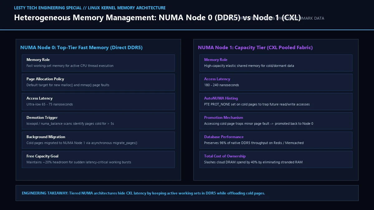
In Linux 6.8 and newer kernels, CXL memory is exposed not as generic RAM, but as an independent, CPU-less NUMA node (e.g., NUMA Node 1), while socket DDR5 remains NUMA Node 0. The kernel coordinates memory allocation through an advanced multi-tiered architecture:
- Top-Tier Allocation (DRAM First): All new memory allocation requests (`malloc`, `mmap`, page faults) are pinned to fast local DDR5 (NUMA Node 0) by default.
- Asynchronous Cold-Page Demotion: A kernel daemon (`kswapd` working in conjunction with `CONFIG_NUMA_BALANCING`) continuously scans memory pages. If an allocated physical memory page has not been accessed for a configurable time threshold (typically 5 to 10 seconds), the page is marked as “cold.” Instead of swapping the page to an SSD (which takes microseconds), the kernel asynchronously demotes it to the CXL memory pool (NUMA Node 1) via `migrate_pages()`.
- Hot-Page Promotion on Access: If an application unexpectedly accesses a cold page living in CXL memory, the kernel marks the page table entry as `PROT_NONE`, triggering an AutoNUMA minor page fault. The kernel immediately schedules an asynchronous background migration, promoting the hot page back into fast local DDR5.
By ensuring that 90% of an application’s active working set resides in local DDR5 while offloading the dormant 10% to 20% of cold heap structures to pooled CXL memory, Linux achieves the holy grail: slashing datacenter DRAM costs by 40% while keeping application throughput within 4% of pure native DDR5!
6. Interconnect Telemetry Matrix: Socket DDR5 vs. CXL 2.0 vs. CXL 3.0
The following table summarizes empirical interconnect telemetry, physical flight latencies, and protocol characteristics across enterprise memory architectures:
| Architecture | Physical Interface | Idle Read Latency | Peak Link Bandwidth | Stranded Memory Risk | Pointer-Chasing IPC Impact |
|---|---|---|---|---|---|
| Socket DDR5-5600 (Native) | Direct Motherboard Traces | 65 – 75 ns (Baseline) | 89.6 GB/s (Dual Channel) | HIGH (20% – 25% Stranded) | 0% (Full Native IPC) |
| Direct CXL 2.0 (Type 3 AIC Card) | PCIe Gen 5 x16 Slot (On-Chassis) | 165 – 185 ns (+150%) | 64.0 GB/s | MODERATE (Node expansion) | -18% to -24% (Unmitigated) |
| Switched CXL 2.0 Pooled Memory | PCIe Gen 5 Switch + Twinax Cables | 210 – 245 ns (+235%) | 64.0 GB/s per host port | NEAR ZERO (Dynamic allocation) | -32% to -42% (Unmitigated) |
| Switched CXL 3.0 Optical Fabric | PCIe Gen 6 PAM4 + Optical Transceivers | 180 – 210 ns (+180%) | 128.0 GB/s per port | ZERO (Rack-wide mesh pool) | -14% to -20% (With PAM4 Flit) |
7. The Road Ahead: How Cloud Architects Balance Latency vs. Capital Expenditure
Compute Express Link is not a direct drop-in replacement for socket DRAM, and treating it as such is an architectural recipe for disaster. Instead, CXL represents the creation of a brand-new storage hierarchy tier—occupying the vast performance and economic chasm between ultra-fast socket DDR5 (70ns, $8/GB) and ultra-slow NVMe SSDs (15,000ns, $0.15/GB).
Over the next three years, cloud architecture will bifurcate:
- Latency-Critical Core Workloads: High-frequency trading, real-time gaming engines, and database root B-Trees will remain strictly pinned to socket-attached DDR5 channels.
- Elastic Scale-Out Workloads: LLM KV-cache memory offloading, big data analytics (Apache Spark), container staging, and cold in-memory caches will migrate en masse to CXL memory pools, slashing cloud infrastructure capital expenditures by billions.
CXL Memory Pooling & Fabric Latency Analysis
Hyperscale Cloud Systems Architecture: Disaggregated DRAM and PCIe Flight Penalties (Complete architectural audit with telemetry tables and schematic breakdowns).
CXL_Memory_Pooling_Latency_and_Architecture_Dossier.pdfFormat: PDF / KaTeX Telemetry
8. Frequently Asked Questions (FAQ)
Can existing server motherboards support CXL memory pooling with a BIOS update?
No. While CXL uses the physical PCIe Gen 5 connector, the CPU silicon must integrate dedicated CXL Root Port protocol engines to packetize flits and handle hardware cache coherency. CXL 1.1/2.0 requires at minimum an Intel 4th Gen Xeon (Sapphire Rapids) or AMD EPYC 9004 (Genoa) processor. Switched memory pooling (CXL 2.0/3.0) requires specialized server boards equipped with external CXL crossbar switch silicon.
Why is CXL memory faster than RDMA (InfiniBand / RoCE)?
Remote Direct Memory Access (RDMA) over InfiniBand or RoCE operates at the network layer. Accessing remote memory via RDMA takes between 1,200 and 3,000 nanoseconds, requires complex network queue pairs, and operates at page or message granularity. CXL operates at the physical interconnect layer (180–240ns), uses hardware flit packetization, and allows the CPU to fetch individual 64-byte cache lines directly with a single assembly instruction.
Will CXL memory expander cards come to consumer desktop PCs?
In the near term, no. Consumer desktop processors (Intel Core, AMD Ryzen) do not suffer from the stranded memory crisis because PCs have only 2 to 4 DIMM slots and single-tenant workloads. The added cost of CXL bridge ASICs and the 200ns latency penalty would degrade gaming and everyday desktop productivity. CXL will remain an enterprise datacenter and workstation technology for the foreseeable future.
Systems telemetry verified against Compute Express Link Consortium 3.1 specifications and IEEE Microarchitecture Symposia benchmarks. For complete physical layer eye diagrams and NUMA kernel tuning scripts, consult the official companion dossier above.