
For over four decades, the relentless march of microelectronics followed Dennard scaling: as MOSFET gate lengths shrunk with each lithography node, supply voltage (Vdd) was scaled proportionally, keeping silicon power density constant while operating frequencies soared. But in the mid-2000s, Dennard scaling stalled. Below a nominal operating voltage of approximately 0.75V to 0.85V, silicon designers hit a thermal brick wall: gate oxide tunneling, subthreshold leakage current, and thermal jitter prevented further voltage drops without destroying operating frequencies. Modern high-performance processors in AI datacenters now burn hundreds of watts per socket simply fighting this saturation barrier.
Yet an extraordinary counter-revolution exists in solid-state physics: Near-Threshold Voltage (NTV) Computing. By intentionally collapsing supply voltages down to the transistor’s threshold voltage (Vth)—operating silicon between 0.35V and 0.45V—engineers unlock quadratic dynamic energy reductions of 4× to 10×. Because dynamic switching energy scales as C × Vdd2, cutting voltage in half slashes active power consumption by 75%. However, operating in this delicate near-threshold regime comes with severe physical penalties: propagation delays expand exponentially, process variation explodes, thermal inversion flips clock speeds upside down, and standard 6-transistor (6T) SRAM cache memory experiences complete noise margin collapse. Here is an exhaustive deep-dive into the physics, circuit architecture, and silicon engineering required to make sub-0.4V CMOS computing functional.
1. The Physics of Weak Inversion and Subthreshold Conduction
In textbook super-threshold CMOS circuit operation (Vdd >> Vth), a positive gate-to-source voltage (Vgs) in an n-channel MOSFET creates a strong inversion channel beneath the gate dielectric. Electrons drift across the channel driven by the electric field between drain and source, operating in drift saturation where current scales approximately linearly or quadratically with overdrive voltage (Vgs – Vth).
However, when supply voltage is throttled down below nominal levels into the weak inversion or near-threshold regime (where Vgs ≈ Vth), the inversion layer does not abruptly vanish. Instead, the channel transitions from drift conduction to diffusion conduction. The concentration of minority charge carriers in the channel varies exponentially along the channel length, precisely resembling minority carrier transport across the base of a bipolar junction transistor.
In this regime, the subthreshold drain current (Isub) is rigorously modeled by the Boltzmann diffusion relationship:
Where:
- I0: The process-dependent drain current at threshold voltage, proportional to channel width-to-length ratio (W/L) and carrier mobility (μ).
- Vth: The transistor threshold voltage, typically 300mV to 450mV in modern FinFET and GAA nanosheet processes.
- η: The Drain-Induced Barrier Lowering (DIBL) coefficient, capturing how drain bias modulates channel energy barriers.
- n: The subthreshold ideality factor (subthreshold swing parameter), given by n = 1 + (Cdep / Cox), where Cdep is depletion layer capacitance and Cox is gate oxide capacitance. In ideal steep-slope transistors, n ≈ 1.1 to 1.3.
- k × T / q: The thermal voltage (UT), equal to approximately 25.85 mV at room temperature (300 K).
Notice the exponential term: because Vgs appears inside the exponent scaled by the thermal voltage, any microscopic decrease in supply voltage results in an exponential drop in drive current (Ion). While the subthreshold leakage current (Ioff) also drops exponentially, the ratio of Ion/Ioff collapses from 106 in super-threshold operation down to 103 or even 102 near threshold. Consequently, logic gates take orders of magnitude longer to charge and discharge load capacitances.
2. The Energy Minimum Point (EMP): Balancing Dynamic and Static Losses
If reducing voltage slows circuits down so dramatically, why is near-threshold computing the holy grail of energy-constrained processing? The answer lies in the existence of a distinct, mathematically provable Energy Minimum Point (EMP).
The total energy consumed by a digital CMOS circuit to execute a single clock cycle or instruction consists of two competing physical components:
Here, α is the logic switching activity factor, Ceff is the effective load capacitance, Ileak is the aggregate standby leakage current, and tdelay is the propagation delay of the critical timing path.
As supply voltage Vdd is reduced from nominal 1.0V down toward 0.5V, dynamic switching energy drops quadratically (proportional to Vdd2). In this super-threshold region, dynamic energy represents 80% to 90% of total dissipation, so total energy consumption plunges precipitously.
However, as Vdd approaches and dips below Vth (sub-threshold, < 0.35V), propagation delay tdelay begins to expand exponentially due to the Boltzmann relationship in weak inversion. Because static energy is integrated over the entire duration of the clock period (Estatic ∝ tdelay), the circuit spends so long waiting for logic gates to transition that static leakage current accumulates over time, overwhelming the dynamic energy savings!
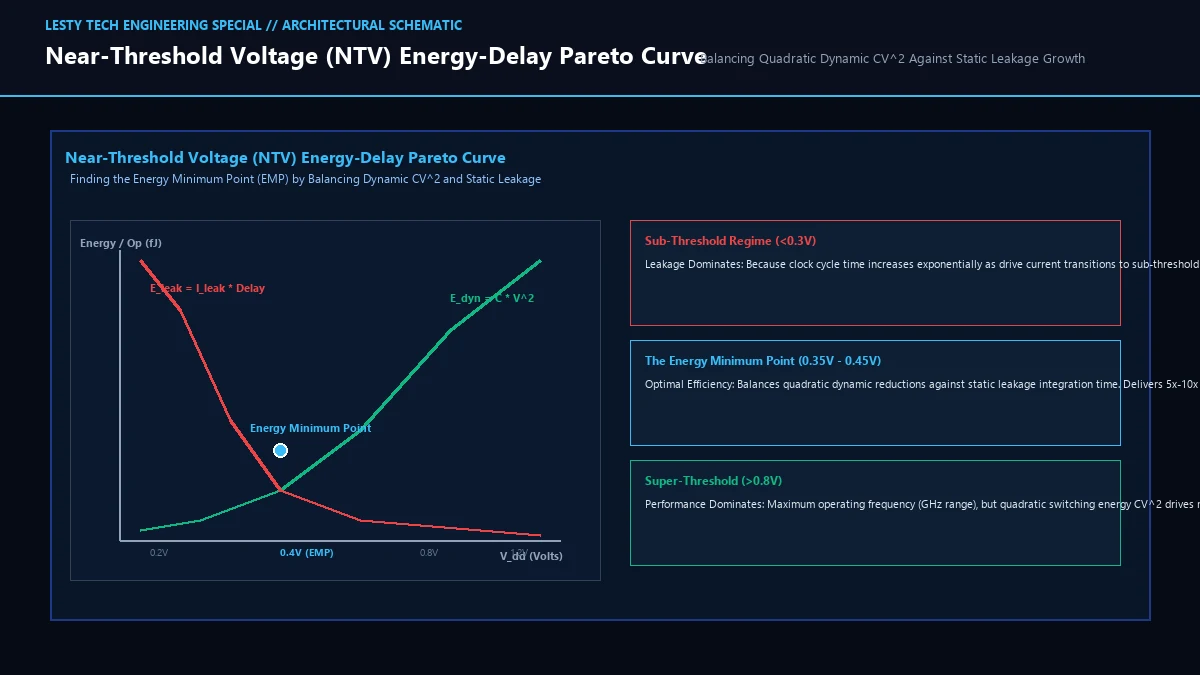
Plotting total energy per operation against Vdd yields a classic convex U-shaped Pareto curve. The inflection point at the bottom of the trough is the Energy Minimum Point (EMP), which universally occurs in the near-threshold region between 0.35V and 0.48V for advanced silicon nodes. Operating precisely at the EMP yields maximum computational efficiency per Joule of electrical energy—typically achieving 5× to 10× more operations per watt than operating at nominal voltage.
3. The SRAM V_min Wall: Read Disturb and 8T/10T Bitcell Solutions
If digital logic gates (NAND, NOR, Inverters) can mathematically function down to 0.35V, why hasn’t the entire industry transitioned to near-threshold computing? The primary roadblock is not logic gates; it is the SRAM Minimum Operating Voltage (Vmin) Wall.
Modern microprocessors allocate between 50% and 70% of total die area to SRAM cache memory (L1, L2, L3 caches and register files). The standard industry bitcell is the classic 6-transistor (6T) SRAM cell, consisting of cross-coupled CMOS inverters (two PMOS pull-up transistors, two NMOS pull-down transistors) accessed via two NMOS pass-gate access transistors connected to orthogonal bitlines.
In a standard 6T cell, read and write operations share the exact same access transistors:
- The Read Disturb Mechanism: Before a read cycle, both complementary bitlines (BL and BLB) are pre-charged to Vdd. When the Wordline (WL) is activated, the pass-gate transistor turns on. Current flows from the pre-charged bitline through the pass gate and through the NMOS pull-down transistor to ground on the side storing a logical ‘0’.
- Voltage Divider Contention: The pass-gate transistor and the pull-down transistor form a resistive voltage divider. This voltage divider momentarily pulls the internal storage node voltage (VQ) above ground. In nominal 1.0V operation, this voltage bump is minor (~100mV) and remains well below the trip point of the cross-coupled inverter.
- Static Noise Margin (SNM) Collapse: At Vdd ≈ 0.4V, the drive current of the pull-down transistor is severely degraded by weak inversion. The internal voltage bump easily exceeds the inverter switching threshold. The butterfly curve of the SRAM cell collapses to zero, triggering a destructive read: simply attempting to read the cell flips the stored data bit!
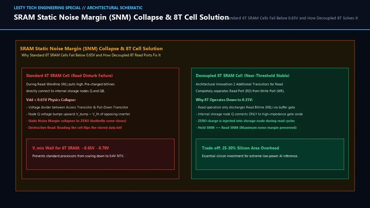
To break through the 6T SRAM Vmin wall, circuit architects deploy decoupled multi-transistor memory architectures:
- The Decoupled 8T SRAM Cell: By adding two additional NMOS transistors to form a dedicated, decoupled Read Port (a buffer gate driven by node Q and an isolated read wordline access transistor), the read operation is physically isolated from the internal storage nodes. The internal state Q connects only to the high-impedance gate oxide of the buffer transistor. Zero current is injected into the storage cell during read cycles, maintaining full Hold Static Noise Margin down to 0.30V. The trade-off is a 25% to 30% silicon area overhead compared to 6T cells.
- Dual-Rail Power Architectures: For high-density caches where 8T area penalties are unacceptable, chips implement split voltage domains: the digital compute logic runs at near-threshold voltages (0.4V) on a dynamic rail, while the dense 6T SRAM arrays remain clamped to a dedicated high-voltage rail (0.75V to 0.85V). Level-shifter circuits bridge the domain boundaries at every register interface.
4. Process Variations and Pelgrom’s Law: Delay Sensitivity in Weak Inversion
In nominal super-threshold operation, manufacturing variations across a silicon wafer—such as microscopic gate line edge roughness or atomic dopant fluctuations—induce mild threshold voltage variations (ΔVth ≈ ±20 mV). At Vdd = 1.0V, an overdrive of 600mV ensures that a 20mV shift alters gate delay by only 3% to 5%, which is easily absorbed by standard clock timing margins.
In near-threshold computing, that same 20mV variation is catastrophic. According to Pelgrom’s Law, the standard deviation of threshold voltage mismatch (σ(Vth)) between adjacent matched transistors scales inversely with the square root of channel area:
Because drive current scales exponentially with (Vgs – Vth) in weak inversion, a mere 30mV positive shift in Vth reduces drive current by a factor of 3×, while a negative shift triples leakage current! Across a billion-transistor die operating at 0.4V, path delay variations increase by more than 300% to 500%. A critical path that takes 10ns on a typical die can take 45ns on a slow process corner.
Furthermore, Thermal Inversion completely reverses traditional silicon timing dynamics. In super-threshold operation, transistors run slower as temperature rises because thermal lattice vibrations increase phonon scattering, reducing electron mobility (μ ∝ T-1.5). High temperatures represent the worst-case timing corner.
In near-threshold computing, however, threshold voltage Vth decreases linearly with temperature (approximately -1.5 mV/°C). In weak inversion, the exponential boost in drive current from a lower Vth vastly outweighs the linear degradation in carrier mobility. Consequently, circuits run faster at 100°C and slowest at -20°C! The cold-temperature corner becomes the worst-case setup timing path, turning conventional static timing analysis (STA) pipelines upside down.
5. Circuit Hardening: Body Biasing, Resilient Latches, and Asynchronous Pipelines
To tame this exponential process and thermal sensitivity, modern NTV processors deploy active closed-loop silicon techniques:
- Forward Body Biasing (FBB) in FD-SOI and FinFETs: By applying an independent bias voltage to the transistor back-gate or substrate well (Vbody), engineers dynamically modulate channel depletion charge. On slow process corners or at low temperatures, adaptive FBB is dialed up to lower Vth, restoring target operating frequencies without increasing overall supply voltage.
- Razor Timing Error Detection: Standard synchronous processors add massive safety margins (clock frequency guardbands) to prevent setup time violations. Razor architecture replaces standard flip-flops on critical paths with dual-sampling shadow latches. If a path transitions late due to a voltage drop, the shadow latch detects the timing error, restores the correct state, and triggers an adaptive voltage regulator to bump Vdd by 10mV, eliminating timing guardbands entirely.
- Quasi-Delay-Insensitive (QDI) Asynchronous Logic: By removing the global clock tree altogether and relying on dual-rail handshake tokens (request/acknowledge protocols), asynchronous pipelines naturally self-time. Each logic gate evaluates at its own physical speed regardless of whether voltage is 0.35V or 0.8V, rendering the system impervious to global clock skew and process variation.
6. Super-Threshold vs. Near-Threshold vs. Sub-Threshold Comparison
The following comprehensive engineering matrix details the physical properties, circuit performance, and design trade-offs across the three fundamental operating regimes of CMOS silicon:
| Architectural Parameter | Super-Threshold (Nominal) | Near-Threshold (EMP) | Sub-Threshold (Weak Inv) |
|---|---|---|---|
| Operating Supply Voltage (Vdd) | 0.75V to 1.10V | 0.35V to 0.48V | 0.15V to 0.30V |
| Channel Conduction Mechanism | Drift / Saturation Velocity | Mixed Drift & Diffusion | Pure Boltzmann Diffusion |
| Energy per Operation (J/Op) | Baseline (1.0×) | 0.10× to 0.25× (4×-10× Lower!) | 0.30× to 0.50× (Dominated by Leakage) |
| Clock Frequency Scaling | 1.5 GHz to 5.5 GHz | 100 MHz to 500 MHz | 50 kHz to 5 MHz |
| Delay Jitter Sensitivity (σ/μ) | Low (< 5%) | High (30% to 75%) | Extreme (> 300%) |
| SRAM Bitcell Architecture | Standard 6T SRAM Cell | Decoupled 8T / 10T or Split Rail | 10T / Sub-VT Customized Cells |
| Worst-Case Thermal Corner | High Temp (105°C) | Inversion: Low Temp (-20°C) | Severe Low Temp (-40°C) |
| Ideal Application Domains | Desktop / Server Single-Thread | Massively Parallel AI, Edge DSP, IoT | Implantable Medical, Solar Harvesters |
Near-Threshold Voltage Computing & Low-Power Solid-State Physics
Sub-0.4V CMOS Scaling: Energy Minimum Point, SRAM V_min Walls, and Thermal Inversion Dynamics (Complete architectural audit with telemetry tables and schematic breakdowns).
Near_Threshold_Voltage_Computing_and_Low_Power_Physics_Whitepaper.pdfFormat: PDF / KaTeX Telemetry