In the architecture of large language models, the standard multi-head self-attention mechanism scales quadratically with sequence length: O(N2) in both compute and memory. In 2022, Tri Dao and the Stanford Hazy Research lab shattered this computational memory wall with FlashAttention, introducing tiled online softmax to compute exact attention without materializing massive intermediate attention matrices in high-bandwidth memory (HBM). FlashAttention-2 followed in 2023, parallelizing outer loops and optimizing work partitioning across Streaming Multiprocessors (SMs) on NVIDIA Ampere GPUs.
However, when FlashAttention-2 was deployed on NVIDIA’s next-generation Hopper H100 architecture, silicon utilization plateaued at roughly 35% to 50% of peak theoretical floating-point performance. Despite the H100 boasting groundbreaking hardware units like the Tensor Memory Accelerator (TMA) and asynchronous Warp Group Matrix Multiply and Accumulate (WGMMA), existing CUDA attention kernels were trapped in synchronous execution patterns: compute threads constantly stalled waiting on global memory loads, and tensor cores sat idle while scalar ALUs computed softmax normalization.
Enter FlashAttention-3. By re-architecting the attention algorithm from the silicon up, Dao and team achieved an unprecedented 850 TFLOPS FP8 throughput and 660 TFLOPS FP16 throughput on a single NVIDIA H100 GPU—saturating up to 75% to 85% of theoretical silicon limits. The breakthrough relies on three foundational innovations: Hardware Warp Specialization, Asynchronous TMA Multistage Circular Buffering, and GEMM-Softmax Compute Overlapping. Here is the definitive deep-dive into how FlashAttention-3 harnesses Hopper silicon physics.
1. The Hopper Microarchitectural Leap: TMA and WGMMA
To understand why FlashAttention-2 hit a performance ceiling on Hopper, one must examine the fundamental architectural divergence between NVIDIA’s Ampere (A100) and Hopper (H100) GPUs:
- Ampere Load-Compute Coupling: On A100, moving a tile of data from global HBM memory into Shared Memory (SRAM) required general-purpose CUDA threads to execute explicit memory instructions (
LDG) into registers, followed by shared memory store instructions (STS). This burned hundreds of register file entries per thread and forced warp schedulers to execute address calculations instead of matrix math. Even with Ampere’s asynchronous copy feature (cp.async), threads still managed address pipelines and synchronizations. - Hopper Tensor Memory Accelerator (TMA): Hopper introduced a dedicated hardware engine located inside each SM called the TMA. TMA takes a multidimensional tensor descriptor in global memory and autonomously streams 2D, 3D, or 5D tiles directly into Shared Memory without involving CUDA cores or touching the register file! A single thread issues a single TMA descriptor instruction, and the hardware DMA engine transfers the entire matrix tile asynchronously.
- Asynchronous WGMMA (Warp Group MMA): In Ampere, matrix multiply instructions (
mma.sync) required all 32 threads in a warp to hold matrix fragments in their register files and wait synchronously for the tensor core to finish. Hopper introduced WGMMA, where an entire group of four warps (128 threads) cooperatively issues a matrix multiply instruction that reads input operands directly from Shared Memory into Tensor Cores asynchronously, writing results into accumulator registers while threads continue other work.
2. Hardware Warp Specialization: Producer vs. Consumer Roles
In FlashAttention-2, every warp in a threadblock was homogeneous: all warps loaded data from HBM into shared memory, all warps participated in matrix multiplication, and all warps calculated row-wise softmax exponentials and sums.
This homogeneous structure caused severe warp pipeline bubbles on Hopper. When warps were loading data or waiting on memory barriers, the H100’s fourth-generation Tensor Cores sat starved of data. Conversely, when warps were executing matrix math, the memory bus went underutilized.
FlashAttention-3 dismantles this paradigm using Hardware Warp Specialization. A threadblock of 128 or 256 threads is partitioned into two physically distinct functional groups:
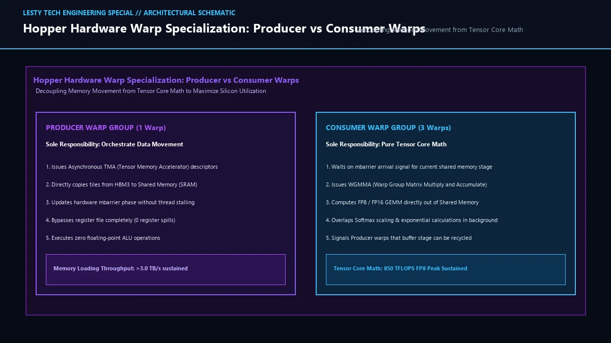
- The Producer Warp Group (1 Warp, 32 Threads): The producer warp is dedicated solely to memory orchestration. It never touches tensor arithmetic or floating-point operations. Its job is to calculate global memory addresses, issue asynchronous TMA descriptor loads to stream incoming Key (K) and Value (V) tiles into Shared Memory, advance hardware barrier phases, and manage circular shared memory buffers. Because it requires virtually zero registers, it operates with minimal register pressure.
- The Consumer Warp Group (3 to 7 Warps, 96 to 224 Threads): Consumer warps never execute global memory loads. They live in a continuous computational loop: they wait on hardware asynchronous barriers (
mbarrier), execute WGMMA instructions to compute Query-Key dot products (Q × KT), run online softmax normalization, and multiply attention weights by Value tiles (P × V). Consumer warps dedicate their entire register allocation to accumulator registers, enabling maximal math precision and throughput.
By decoupling memory fetching from tensor compute, Producer warps fetch data several pipeline stages ahead of compute, completely hiding HBM3 memory latency behind continuous Tensor Core utilization!
3. Multistage Circular Shared Memory and Asynchronous Barriers
To coordinate Producer and Consumer warps without stalling execution, FlashAttention-3 constructs a multistage circular shared memory pipeline governed by Hopper hardware barriers (mbarrier).
On NVIDIA Hopper, each SM is equipped with 228 KB of Shared Memory (compared to 164 KB on Ampere). FlashAttention-3 carves this SRAM into multiple circular buffer stages (typically 3 or 4 stages):
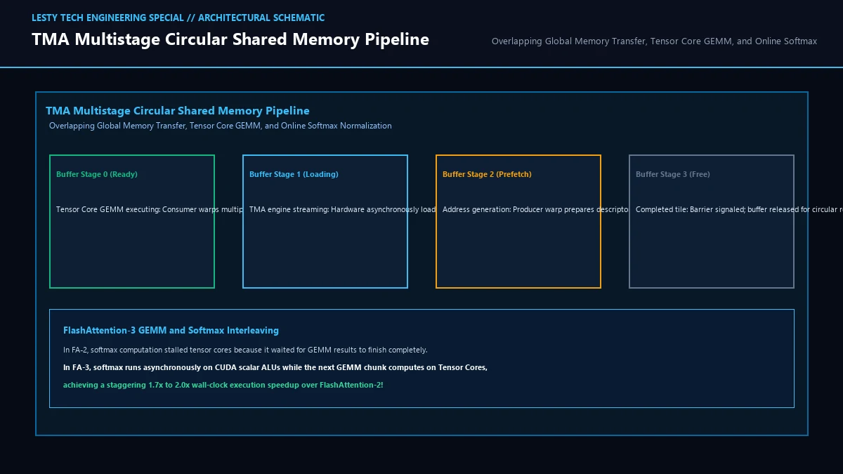
The lifecycle of each circular stage operates through hardware transaction barriers:
- Phase 1 (Producer Arrival): The Producer warp issues a TMA transfer for Stage S and initializes an asynchronous transaction barrier with the expected byte count (e.g.,
mbarrier.init.shared::ctawith 32 KB). As TMA hardware writes bytes from HBM3 directly into the stage buffer, it automatically decrements the hardware barrier counter. - Phase 2 (Asynchronous Completion): When the last byte lands in SRAM, the hardware flips the barrier phase bit. Crucially, zero CPU or GPU thread cycles are burned polling or waiting.
- Phase 3 (Consumer Execution): Consumer warps execute
mbarrier.try_wait.parity.shared::cta. As soon as the phase bit flips, consumer warps immediately dispatch WGMMA instructions directly reading from Stage S. - Phase 4 (Buffer Recycling): Once Consumer warps finish reading Stage S, they signal a release barrier. The Producer warp, which has already been prefetching Stage S+1 and Stage S+2, recycles Stage S for the next block iteration.
This ping-pong circular buffering ensures that at any given microsecond, one buffer stage is actively feeding Tensor Cores, another stage is being filled by TMA over the 3.0 TB/s HBM3 bus, and a third stage is being address-resolved. Pipeline stalls are mathematically eradicated.
4. PTX Assembly Mechanics and Shared Memory Swizzling
Under the hood, FlashAttention-3’s performance advantage is forged in low-level Parallel Thread Execution (PTX) assembly. Understanding the exact instructions reveals how hardware boundaries are navigated:
Asynchronous Bulk Tensor Copies: The Producer warp invokes the specialized Hopper instruction:
This single instruction instructs the TMA hardware to look up the tensor descriptor, compute 2D matrix stride offsets, stream bytes across high-speed on-chip interconnects directly into Shared Memory, and notify the hardware barrier %mbar_ptr upon completion—all with zero register usage.
Bank Conflict Elimination via XOR Swizzling: Shared memory on Hopper is divided into 32 independent banks with a 4-byte bandwidth per cycle. In high-dimensional FP8 and FP16 GEMM operations, naive row-major or column-major memory layouts cause multiple threads in a warp group to request bytes from the same shared memory bank simultaneously, generating devastating 32-way bank conflicts that serialize memory access. FlashAttention-3 implements non-linear XOR address swizzling: the column index bits are XOR-ed with row index bits before storing tiles into SRAM. This mathematical permutation guarantees that 128-byte contiguous memory loads hit completely disjoint banks, delivering the theoretical maximum 14.5 TB/s shared memory bandwidth per SM!
5. Overlapping GEMM and Online Softmax Normalization
Even with Warp Specialization and TMA, FlashAttention-2 suffered from a hidden microarchitectural bottleneck: the alternating dependency between GEMM and Softmax.
In FlashAttention, computing self-attention requires three sequential mathematical phases per block:
- GEMM-1: Compute S = Q × KT (Matrix multiplication on Tensor Cores).
- Softmax: Compute row-wise maximums, exponents (exp(S – m)), and normalization sum l (Vector math on CUDA scalar/SFU ALUs).
- GEMM-2: Compute O = P × V (Matrix multiplication on Tensor Cores).
In FlashAttention-2, these phases were strictly serialized: Tensor Cores computed GEMM-1, then sat completely idle while CUDA scalar cores computed exp() and division, and only then resumed to compute GEMM-2. Because scalar core throughput is drastically lower than Tensor Core throughput (Hopper has 16× more Tensor FLOPs than scalar ALU FLOPs), this non-matmul phase created massive silicon bubbles.
FlashAttention-3 solves this by pipelining and overlapping GEMM and Softmax across consecutive blocks. While Consumer Warps are calculating the online softmax scaling for block i on the SM’s Special Function Units (SFUs) and ALUs, the Tensor Cores are concurrently executing the asynchronous WGMMA instructions for GEMM-1 of block i+1!
Because WGMMA writes its results asynchronously to accumulator registers without blocking other execution pipes, the CUDA scalar cores and Tensor Cores run concurrently in full hardware parallelism.
6. FP8 Precision Scaling: Conquering Quantization Noise in Attention
The ultimate performance frontier in FlashAttention-3 is native support for 8-bit floating-point (FP8) execution, pushing Hopper H100 throughput past 850 TFLOPS.
However, quantizing self-attention to FP8 is notoriously perilous. While linear layers (FFNs) tolerate quantization well, attention matrices contain extreme activation outliers: when dot products Q × KT are scaled, exponential softmax operations amplify tiny numerical errors, causing attention weights to collapse or explode.
FlashAttention-3 overcomes FP8 quantization noise through three rigorous mathematical techniques:
- Incoherent Matrix Transformation: Prior to GEMM, Q and K matrices are multiplied by a randomized Hadamard orthogonal matrix. This spreads activation outliers evenly across all hidden dimensions, eliminating isolated high-magnitude spikes without altering the mathematical inner product.
- Per-Block Dynamic Scaling: Rather than using a coarse per-tensor static scale factor, FlashAttention-3 calculates dynamic FP8 scale factors on-the-fly for every individual Shared Memory tile block (typically 64×128). This preserves the full dynamic range of the FP8 format (E4M3: 1 sign bit, 4 exponent bits, 3 mantissa bits).
- FP32 Accumulation in Shared Memory: While input operands K, Q, and V are stored in FP8 to double memory bandwidth, all intermediate dot products and softmax normalizations are accumulated strictly in full 32-bit floating-point (FP32) inside Tensor Core registers, guaranteeing exact mathematical equivalence with baseline FP16 implementations.
7. Generational Architectural Comparison: FlashAttention-1 vs 2 vs 3
The following table outlines the architectural evolution of the FlashAttention kernel family across three generations of GPU hardware:
| Architectural Dimension | FlashAttention-1 (2022) | FlashAttention-2 (2023) | FlashAttention-3 (2024-2026) |
|---|---|---|---|
| Target GPU Architecture | Ampere (A100) / Turing | Ampere / Ada Lovelace | Hopper (H100/H200) & Blackwell |
| Peak FP16 TFLOPS (H100) | ~220 TFLOPS | ~380 TFLOPS | 660 to 720 TFLOPS |
| FP8 Tensor Core Throughput | Unsupported | Experimental (~450 TFLOPS) | 850+ TFLOPS Sustained |
| Memory Movement Engine | CUDA Core LDG/STS instructions | cp.async (Ampere async copy) | Asynchronous TMA (Direct HBM-SRAM) |
| Warp Execution Structure | Homogeneous (All warps compute) | Homogeneous with outer loop tiling | Hardware Warp Specialization (P/C) |
| GEMM & Softmax Coordination | Synchronous serialization | Reduced non-matmul FLOPs | Pipelined Interleaved Overlap |
| Silicon Efficiency (% Peak H100) | ~25% | ~45% | 75% to 85% Theoretical Peak |
FlashAttention-3: Hardware Warp Specialization & FP8 Acceleration
Hopper H100 Silicon Optimization: Asynchronous TMA, Circular Buffering, and GEMM-Softmax Overlap (Complete architectural audit with telemetry tables and schematic breakdowns).
FlashAttention_3_Warp_Specialization_and_FP8_Architecture_Guide.pdfFormat: PDF / KaTeX Telemetry
Frequently Asked Questions About FlashAttention-3
Can FlashAttention-3 run on consumer GPUs like the RTX 4090 or older A100s?
wgmma.mma_async, and hardware transaction barriers. On RTX 4090 and A100, FlashAttention-2 remains the fastest available implementation.
Does FP8 attention cause perplexity degradation during LLM inference?
How does FlashAttention-3 integrate into production serving frameworks like vLLM and TensorRT-LLM?
torch.nn.functional.scaled_dot_product_attention and has been integrated into both TensorRT-LLM and vLLM. In high-concurrency production inference environments with long context windows (32k to 128k tokens), switching from FA-2 to FA-3 cuts time-to-first-token (TTFT) by 40% to 55% and increases serving throughput by up to 1.8× per H100 node.