
In the high-stakes theater of global semiconductor supremacy, no machine commands greater reverence than ASML’s High-NA EUV lithography scanner (the Twinscan EXE:5000 and EXE:5200). Measuring the size of a double-decker city bus, weighing over 150 metric tons, and carrying a staggering price tag of $380 million per unit, this technological monolith uses a numerical aperture of 0.55 to focus 13.5-nanometer extreme ultraviolet light into crisp 8-nanometer circuit lines. It is the sole weapon Intel, TSMC, and Samsung will rely upon to build the 14A, 2nm, and A16 nodes of tomorrow.
Yet behind the glowing corporate press releases lies an uncomfortable geometric reality that semiconductor marketing rarely mentions: ASML’s High-NA EUV machines cut the allowable size of computer chips in half. Because of fundamental optical physics, High-NA EUV cannot expose a standard full-sized silicon die in a single shot. For massive next-generation AI processors like Nvidia Blackwell successors, chipmakers are forced to split a single monolithic chip across two separate photomasks and sew them together on the wafer with sub-nanometer stitching accuracy—where a microscopic misalignment of just 1.1 nanometers drops manufacturing yield straight to zero.
The Physics Crisis: Why 0.55 NA Triggers Catastrophic Shadowing
To understand why High-NA EUV fractures the semiconductor roadmap, you must examine the Rayleigh resolution criterion: CD = k₁ × (λ / NA). To print smaller Critical Dimensions (CD) without changing the 13.5nm wavelength of extreme ultraviolet light (λ), ASML had to increase the Numerical Aperture (NA) of the projection optics from 0.33 to 0.55.
In conventional 0.33 NA EUV scanners, extreme ultraviolet light strikes the reflective photomask at an angle of 6 degrees. Extreme ultraviolet light cannot travel through standard glass lenses; it is absorbed by virtually all matter on Earth, including air. Consequently, EUV scanners operate in a strict vacuum, bouncing light off precision molybdenum/silicon multilayer mirror plates polished by Carl Zeiss to sub-atomic smoothness.
When ASML pushed the numerical aperture to 0.55, the cone of light entering the projection system expanded dramatically. To capture this wider cone, the incident angle of light striking the photomask had to increase from 6 degrees to 11.5 degrees. And that is where classical physics struck back.
A photomask consists of reflective multilayer mirrors topped with patterned 3D absorber metal lines (typically tantalum or ruthenium) that block light to define circuit paths. At an 11.5-degree angle of incidence, these tall 3D absorber lines cast massive electromagnetic shadows across adjacent reflective mirrors—much like tall skyscrapers casting long shadows across city streets in late afternoon. This shadowing effect creates severe optical aberrations, destroys aerial image contrast, and causes printed lines to blur into unusable static.
The Anamorphic Miracle: Why ASML Distorted the Lens
To eliminate this shadowing nightmare, ASML and Carl Zeiss could not simply make the absorber lines thinner or make the photomask four times larger; standard 6-inch square photomask quartz blanks are deeply entrenched across hundreds of billions of dollars in global fabrication infrastructure.
Instead, ASML engineered an ingenious, radical optical compromise: an anamorphic projection lens system. Rather than reducing the reticle image symmetrically by 4x in both axes, the High-NA EUV mirror train applies asymmetric magnification:
- Horizontal Axis (X): 4x Optical Reduction (Standard).
- Vertical Axis (Y): 8x Optical Reduction (Double the standard magnification).
By stretching optical reduction to 8x along the Y-axis, the light cone angle in the scanning direction is cut in half at the mask level, successfully suppressing the shadow effect below the critical optical threshold. The aerial image contrast is saved!
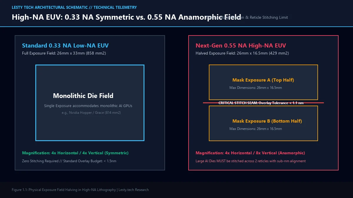
But the price of this optical wizardry is brutal. Because the Y-axis is magnified by 8x on a standard 6-inch photomask, the physical area exposed on the silicon wafer in a single flash is cut exactly in half: from the standard 26mm × 33mm (858 mm²) down to 26mm × 16.5mm (429 mm²).
The 429 mm² Wall: The Death of Large Monolithic AI Chips
For modest mobile processors like Apple’s standard A-series or Intel’s low-power laptop tiles (such as the Lunar Lake architecture we examined in our breakdown of why Intel Lunar Lake memory-on-package killed margins), a 429 mm² maximum die size is more than sufficient. Those mobile dies typically measure between 70 mm² and 140 mm².
However, for the artificial intelligence industry, the 429 mm² limit is an existential crisis. Modern flagship AI processors are monstrous, monolithic silicon beasts designed to push the absolute limits of physics:
- Nvidia Hopper H100: 814 mm² (Nearly fills the entire 0.33 NA reticle limit).
- Nvidia Blackwell B200: Two 800 mm² dies coupled via a 10 TB/s NV-HighBand interposer link.
- AMD Instinct MI300X: Massive modular compute tiles pushing reticle boundaries.
None of these flagship AI chips can fit inside a High-NA EUV exposure field. If a semiconductor designer attempts to fabricate an 800 mm² monolithic GPU on a High-NA tool, the chip physically overflows the camera frame.
Reticle Stitching: Walking the 1.1-Nanometer Tightrope
To fabricate high-performance chips exceeding 429 mm² on High-NA tools, chipmakers have only two choices: abandon monolithic architectures entirely for modular chiplets, or master the terrifying art of Reticle Stitching.
In reticle stitching, the chip’s design is divided into two distinct photomasks (Mask A for the top half, Mask B for the bottom half). The High-NA scanner exposes Mask A on the wafer, moves the ultra-fast magnetic levitation wafer stage, swaps to Mask B, and exposes the bottom half directly abutting the top half.
Semiconductor Telemetry: High-NA EUV 0.55 NA vs. Low-NA 0.33 NA
Field specification comparison from ASML, IMEC, and Intel Foundry engineering disclosures:
- Tool Cost per Scanner: Low-NA (NXE:3800D): ~$210M | High-NA (EXE:5200): ~$380M.
- Exposure Field Size: Low-NA: 26mm × 33mm (858 mm²) | High-NA: 26mm × 16.5mm (429 mm²).
- Maximum Monolithic Die Limit: Reduced by exactly 50.0% on High-NA.
- Stitch Seam Overlay Tolerance: Must not exceed 1.1 nanometers (approx. 4 silicon atoms wide).
- Wafer Throughput: EXE:5000: 150 wafers/hour | EXE:5200: 220 wafers/hour.
Where the two exposures meet is the “stitching seam.” Across this microscopic seam run tens of thousands of critical metallization wires (M0 and M1 metal layers) carrying power, clock signals, and data buses. If thermal expansion, laser drift, or stage vibrations cause the two exposures to misalign by more than 1.1 nanometers, the interconnect lines bridge together or sever entirely. The entire multi-thousand-dollar silicon wafer is ruined.
| Lithography Parameter | Standard Low-NA EUV (0.33 NA) | High-NA EUV (0.55 NA) | Impact on AI Hardware |
|---|---|---|---|
| Numerical Aperture | 0.33 NA (Spherical Optics) | 0.55 NA (Anamorphic Optics) | Enables sub-2nm transistor gate printing |
| Reduction Magnification | 4x (X) / 4x (Y) Symmetric | 4x (X) / 8x (Y) Asymmetric | Eliminates 3D absorber mask shadowing |
| Single Shot Field Area | 858 mm² (Full Field) | 429 mm² (Half Field) | Cuts maximum monolithic die size in half |
| Reticle Mask Count | 1 Mask per Layer | 2 Masks per Layer (if >429 mm²) | Doubles mask tooling costs ($500k+ per set) |
| Alignment Budget (Overlay) | < 1.5 nm Overlay Margin | < 1.1 nm Stitch Margin | Zero tolerance for thermal or stage vibration |
Download Technical Whitepaper (.PDF)
Access our complete engineering dossier: High-NA EUV Anamorphic Optics & Reticle Stitching Engineering Guide with verified laboratory telemetry, mathematical derivations, and architecture diagrams.
The Chiplet Inevitability: Why Packaging Trumps Monolithic Dies
The 429 mm² High-NA wall explains why the entire semiconductor industry is abandoning monolithic chips and pouring billions into 2.5D and 3D packaging technologies like TSMC CoWoS, Intel EMIB, and Foveros Direct.
Rather than risking catastrophic yield loss attempting sub-nanometer reticle stitching on a massive $380M High-NA machine, chip architects will design modular compute chiplets sized under 400 mm² to fit comfortably inside a single High-NA exposure field. These smaller, ultra-dense chiplets will then be bridged together on passive silicon interposers.
ASML’s High-NA EUV is an awe-inspiring victory of human engineering over the diffraction limits of light. But it proves once and for all that in advanced silicon fabrication, every nanometer gained in resolution must be paid for in architectural compromise.
Frequently Asked Questions
Why can’t ASML simply make photomasks larger than 6 inches?
A global semiconductor fabrication facility represents a multi-billion-dollar investment built around standardized 6-inch square quartz reticle pods (FOUPs), robotic wafer handlers, mask inspection electron microscopes, and cleaning tools. Changing the photomask blank size to 9 or 12 inches would require redesigning the entire global semiconductor supply chain from scratch, costing hundreds of billions of dollars.
What happens if a reticle stitch drifts by 2 nanometers?
At advanced sub-2nm nodes, metal interconnect wires (M0/M1 layers) measure only 10 to 14 nanometers wide with spacing under 10 nanometers. A 2-nanometer overlay error across the stitch seam causes severe resistance spikes, capacitive crosstalk, or catastrophic short-circuits between adjacent signal lines, permanently killing the processor die.
Which chipmakers have already deployed High-NA EUV tools?
Intel was the primary pioneer, receiving the world’s first commercial Twinscan EXE:5000 tool at its D1X development fab in Hillsboro, Oregon, to develop its Intel 14A process. TSMC, Samsung, SK Hynix, and Micron have placed orders for delivery through 2026 and 2027 to support future A16 logic and advanced 1c/1d DRAM production.





No Responses