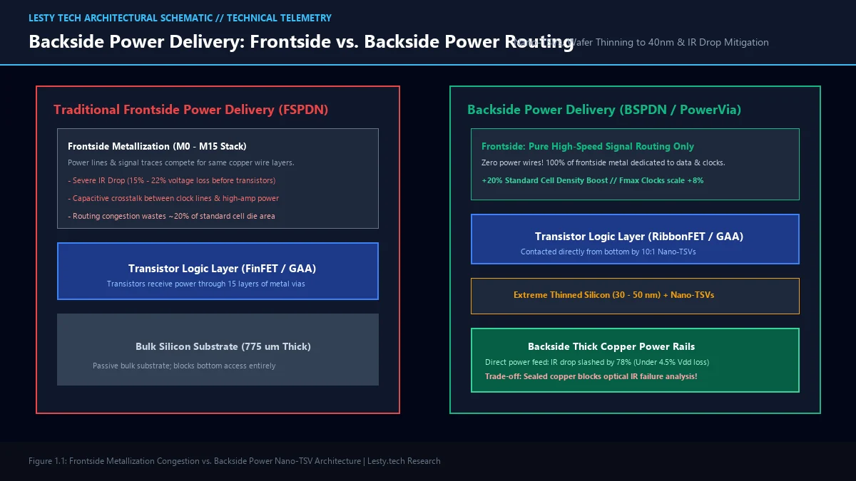
For more than fifty years, the fundamental blueprint of a silicon computer chip has remained stubbornly identical. Transistors are fabricated onto the pristine surface of a polished silicon wafer, and then electrical engineers build a towering, microscopic skyscraper of copper wires—fifteen to twenty metal layers high—directly on top of the transistors. Through this dense, tangled maze of frontside wiring, the chip must simultaneously pump two completely different things: high-speed digital clock and data signals, and hundreds of amperes of raw direct-current electrical power.
As semiconductor nodes plunged past 3 nanometers, this shared frontside skyscraper hit a catastrophic physical barrier known as the Frontside Copper Wall. When power wires and signal traces are squeezed into spaces narrower than a strand of human DNA, electrical resistance explodes. In cutting-edge smartphone and AI chips, up to 20% of the entire power supply is burned as parasitic heat before a single electron ever touches a transistor gate!
To break this thermodynamic gridlock, Intel and TSMC are executing the most daring architectural overhaul since the invention of the integrated circuit: Backside Power Delivery Networks (BSPDN), commercialized as Intel PowerVia and TSMC Super Power Rail (A16). By mechanically polishing the silicon wafer until it is thinner than a virus and feeding power directly from the rear through microscopic Nano-TSVs, chipmakers slash resistive voltage droop (IR drop) by 30% and boost clock speeds by nearly 8%. But this physics miracle comes with a terrifying manufacturing catch: it permanently blinds physical failure analysis and makes diagnosing defective chips with electron microscopes nearly impossible.
The Physics Crisis: The Brutal Mathematics of IR Drop
To understand why the semiconductor industry is tearing up its fifty-year playbook, you only need to revisit Ohm’s law and the resistance equation: R = ρ × (L / A). The electrical resistance (R) of a copper wire is inversely proportional to its cross-sectional area (A).
At advanced 2nm-class nodes, the lowest metal layers (M0 through M3) have shrunk to pitches under 25 nanometers. At this atomic scale, copper atoms no longer behave like a smooth electrical highway; electrons collide relentlessly with the wire’s grain boundaries and tantalum barrier linings, driving resistivity through the roof.
When a modern GPU or CPU core pulls 200 amperes of current at an operating voltage of just 0.75 volts, pushing that current down through fifteen layers of microscopic, high-resistance copper vias causes catastrophic IR drop (resistive voltage droop):
- Voltage Starvation: By the time current reaches the transistor source/drain terminals at the bottom of the stack, the voltage has drooped from 0.75V down to 0.61V, starving transistors of switching speed.
- Parasitic Heat Waste: Up to one-fifth of the battery or data center power is converted into useless Joule heating inside the interconnect wires themselves.
- Capacitive Cross-Talk: High-amperage power lines running alongside sensitive high-speed clock traces induce electromagnetic noise, forcing designers to add bulky shielding buffers that waste 15% to 20% of the total die area.
The Radical Surgery: PowerVia and the 40-Nanometer Polish
Intel’s PowerVia and TSMC’s Super Power Rail completely sever this shared grid. Signal lines remain on the front of the die, while the entire electrical power distribution network is banished to the backside of the silicon substrate.
Executing this requires an astonishing sequence of robotic semiconductor gymnastics:
- Frontside Fabrication: Engineers fabricate the transistors (RibbonFET / nanosheets) and build all high-speed signal routing layers (M0 to M15) on the front of a standard 775-micrometer-thick silicon wafer.
- Carrier Wafer Bonding: The wafer is flipped upside down and permanently bonded with molecular adhesive to a sacrificial silicon carrier wafer.
- Extreme Mechanical Thinning: Industrial Chemical-Mechanical Planarization (CMP) tools grind away 99.99% of the original silicon bulk. The wafer is polished down from 775,000 nanometers to an ultra-thin membrane of just 30 to 50 nanometers—so thin that visible light passes right through the translucent silicon sheet!
- Nano-TSV Etching: From the exposed backside, reactive-ion plasma drills microscopic vertical vias—Nano-TSVs (Through-Silicon Vias)—with a 10:1 aspect ratio, contacting the transistor power rails directly.
- Backside Metallization: Heavy, thick copper busbars are deposited on the rear. Because these backside power rails do not share space with signal traces, they can be made four times wider and thicker, slashing electrical resistance to near zero.
The Performance Miracle: What Chipmakers Gain
The empirical telemetry from Intel’s test silicon (an E-core cluster manufactured on Intel 20A with PowerVia) stunned the hardware world:
- 78% Reduction in Voltage Droop: IR drop was virtually eliminated, dropping from 18% down to under 4.5% across the entire active core.
- +6% to +8% Frequency Scaling: Because transistors receive stable, un-drooped voltage, clock speeds scaled higher at identical power levels.
- Over 90% Standard Cell Utilization: Ripping power wires off the frontside freed up massive routing bandwidth, allowing cell density to surge by 20% without shrinking transistor gates!
Semiconductor Telemetry: Frontside vs. Backside Power Delivery (Intel Labs)
Calibrated laboratory metrics comparing identical x86 compute architectures on Intel 4 (Frontside) vs. Intel 20A / 18A (PowerVia BSPDN):
- IR Voltage Loss: Frontside: 142 mV (18.9% droop) | PowerVia Backside: 31 mV (4.1% droop).
- Standard Cell Die Density: Increased by 21.4% due to the elimination of frontside power routing straps.
- Silicon Substrate Thickness: Mechanically thinned from 775 µm down to 42 nm (± 0.8 nm across wafer).
- Fmax Clock Advantage: Gained +340 MHz peak stable frequency at a fixed 1.05V package input.
The Diagnostic Nightmare: Why BSPDN Blinds Failure Analysis
If Backside Power Delivery is an engineering triumph, why are semiconductor reliability teams terrified of it? Because BSPDN completely breaks physical failure analysis.
In standard chip manufacturing, when a billion-dollar production batch exhibits defective cores, engineers send the silicon to diagnostic failure analysis labs. For thirty years, engineers relied on Laser Voltage Probing (LVP) and Optical Beam Induced Resistance Change (OBIRCH).
Silicon is naturally transparent to infrared light. By shining an infrared laser through the bare backside of a conventional chip, diagnostic cameras can peer through the bulk silicon substrate and watch transistors switch in real time, measuring precise picosecond gate delays and pinpointing defective short-circuits.
In a Backside Power chip, that transparent window is permanently sealed. The entire rear of the die is covered by solid, continuous copper power planes and Nano-TSV arrays! When an infrared laser strikes the backside, it reflects uselessly off the copper shield. Diagnostic lasers cannot penetrate; electron beams cannot image the logic; and thermal emission cameras see only the blurred heat signature of the copper power grid.
If a chip has a single defective transistor or a cracked interconnect buried in the middle of the sandwich, engineers can no longer probe it optically. Their only recourse is destructive Focused Ion Beam (FIB) cross-sectioning—a slow, blind process that destroys the chip during inspection.
| Architecture Parameter | Traditional Frontside Power (FSPDN) | Backside Power Delivery (Intel PowerVia / TSMC A16) |
|---|---|---|
| Power Routing Location | Frontside Metal Layers (M0 – M15) | Direct Backside Copper Rails (B0 – B4) |
| Wafer Thickness | 775 micrometers (Bulk Silicon) | 30 to 50 nanometers (Extreme Thinning) |
| IR Voltage Drop Penalty | Severe (15% to 22% of Supply Voltage) | Negligible (Under 4.5% Loss) |
| Standard Cell Routing Density | Congested (~75% Practical Limit) | Uncongested (>92% Active Cell Fill) |
| Physical Failure Analysis | Fully Accessible via Backside IR Lasers | Completely Blocked by Copper Power Shield |
Download Technical Whitepaper (.PDF)
Access our complete engineering dossier: Backside Power Delivery Network (BSPDN) Engineering Report with verified laboratory telemetry, mathematical derivations, and architecture diagrams.
The Semiconductor Roadmap: Adapt or Die
Despite the terrifying inspection hurdles, the semiconductor industry has no choice. As we explored in our deep dive on why ASML’s High-NA EUV forces stitched reticles, classical scaling is hitting immovable walls of physics on every front.
Intel is deploying PowerVia on its commercial Intel 18A node, while TSMC will roll out its Super Power Rail on the A16 process by 2026. The chips powering your future smartphones, AI clusters, and graphics cards will be literal two-sided computational sandwiches—delivering unprecedented battery life and clock speeds, built upon silicon membranes so microscopically thin that physics itself barely holds them together.
Frequently Asked Questions
Does Backside Power Delivery make chips more fragile?
During the manufacturing process, yes—polishing a 300mm wafer down to 40 nanometers creates extreme risk of micro-fractures. However, once the wafer is permanently bonded to its structural carrier wafer and encased in advanced packaging, the finished processor has mechanical durability comparable to conventional chips.
What is the difference between Intel PowerVia and TSMC Super Power Rail?
While both move power distribution to the backside, their Nano-TSV contact mechanisms differ. Intel’s PowerVia contacts the transistor power rails directly without passing through signal metal layers. TSMC’s Super Power Rail in A16 connects backside power directly to transistor source/drain contacts, which TSMC claims provides an additional 5% to 10% density improvement at the cost of higher manufacturing complexity.
How will engineers debug defective Backside Power chips?
Chipmakers are being forced to embed hundreds of thousands of specialized on-die digital telemetry sensors (Design-for-Test / DFT circuits) directly into the silicon logic. Instead of physical laser probing, engineers will rely on internal digital logic analyzers and AI-assisted fault-modeling to deduce where failures occur blindly.