For more than a decade, the semiconductor industry survived on the back of the 3D FinFET transistor. First commercialized by Intel in 2011 on their 22nm Ivy Bridge architecture and subsequently refined by TSMC and Samsung down to 3nm, the FinFET saved Moore’s Law from catastrophic electrostatic breakdown. By wrapping a conducting gate around three sides of a vertical silicon fin, engineers kept short-channel effects at bay while shrinking gate lengths to microscopic dimensions. But as process geometries punched into the sub-3nm domain, the FinFET ran out of physical runway. At fin widths under 5 nanometers, quantum mechanical tunneling through the fin body triggered massive sub-threshold leakage, gate oxide breakdown, and severe drive-current saturation. The industry’s unanimous salvation was the Gate-All-Around Nanosheet FET (GAAFET)—known variously as RibbonFET at Intel, MBCFET at Samsung, and simply Nanosheet at TSMC. By replacing the vertical fin with vertically stacked, horizontally suspended silicon nanosheet ribbons, the gate electrode completely encloses the channel on all four sides, re-establishing ironclad electrostatic control.
Yet beneath the glowing marketing presentations and multi-billion-dollar fab announcements lies a dirty microscopic secret that nearly derailed sub-2nm commercial yields: sub-channel punch-through leakage into the bulk substrate. While the gate wraps around all four sides of each suspended nanosheet ribbon, the parasitic coupling between the lowest nanosheet channel and the underlying monocrystalline bulk silicon substrate creates an unmitigated leakage highway. In early prototype GAAFET structures lacking substrate isolation, up to 28% of the transistor’s total off-state leakage current bypassed the gate entirely, bleeding current directly into the substrate. To prevent 2nm chips from turning into unmanageable thermal heaters, foundries had to engineer an extraordinarily complex physical barrier: Bottom Dielectric Isolation (BDI). Here is the unvarnished engineering reality of why 2nm nanosheets fail without atomic-layer substrate isolation, how selective isotropic etching makes BDI possible, and the severe thermal phonon penalties that threaten next-generation turbo clock frequencies.
1. The Death of the Fin: Why 3D Silicon Hit an Electrostatic Wall at 3nm
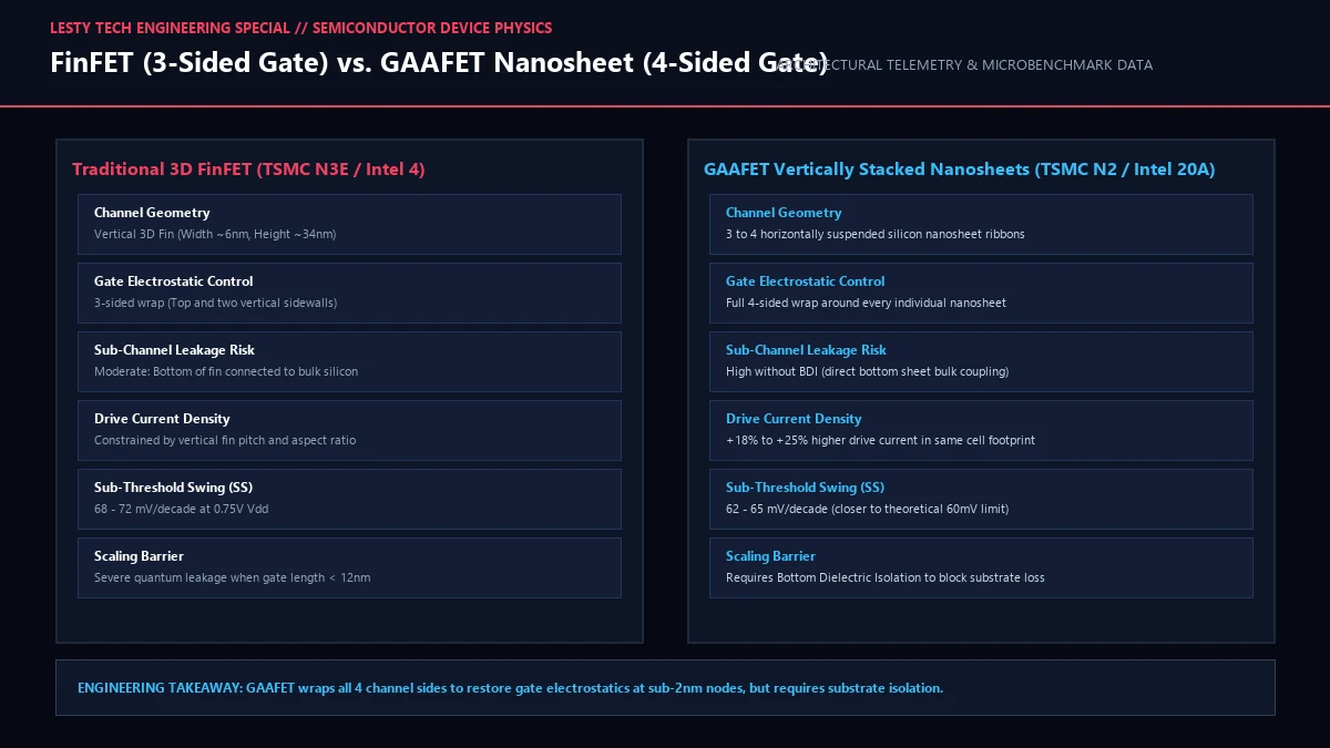
To understand why Bottom Dielectric Isolation is mandatory, one must first appreciate the physical breakdown of the FinFET. In a classic FinFET, the channel consists of a thin vertical slab of silicon rising from the planar substrate. The gate dielectric and metal electrode cover the top surface and the two vertical sidewalls. Electrostatic control is defined by the natural length (λ), derived from Poisson’s equation for a multi-gate architecture:
Where εch is the permittivity of the silicon channel, εox is the permittivity of the gate oxide, tch is the channel fin thickness, and tox is the equivalent oxide thickness (EOT). To maintain an acceptable sub-threshold swing (SS < 70 mV/decade) and suppress Drain-Induced Barrier Lowering (DIBL), the physical gate length (Lg) must be at least four to five times the natural length: Lg ≥ 4.5λ.
At the 3nm node, physical gate lengths compressed down to 12–14nm. To maintain the 4.5λ scaling rule, fab engineers were forced to thin the silicon fin down to an astonishing 4.5 nanometers—equivalent to just 24 silicon atoms across. At this extreme aspect ratio, two fatal physical anomalies occurred:
- Fin Bending and Line Edge Roughness (LER): Ultra-thin vertical fins with aspect ratios exceeding 8:1 suffered mechanical instability during reactive ion etching (RIE) and wet chemical cleaning, leading to physical fin collapse and massive threshold voltage (σVth) variations across the wafer.
- Quantum Confinement Drive Current Collapse: When the fin thickness fell below the de Broglie wavelength of electrons in silicon (~5nm), quantum confinement shifted the sub-band energy levels upward, artificially widening the silicon bandgap and drastically degrading carrier mobility and drive current (Ion).
The FinFET had reached its scaling limit. The only viable path forward was to rotate the channel 90 degrees: stacking multiple horizontal nanosheet ribbons atop one another and routing the gate electrode entirely around every single sheet.
2. Anatomy of a Gate-All-Around Nanosheet: Dimensions, Wires, and Threshold Voltages
In a state-of-the-art GAAFET architecture—such as TSMC’s 2nm (N2) or Intel’s 20A RibbonFET—the active device consists of three or four vertically stacked silicon nanosheets. Each nanosheet is approximately 5 to 6 nanometers in vertical thickness (Tns), 20 to 50 nanometers in horizontal width (Wns), and separated from adjacent sheets by a vertical spacing gap (the inner gate suspension space, Tsus) of approximately 8 to 10 nanometers.
This geometry provides an enormous structural advantage: effective channel width (Weff) scaling. In a FinFET, the effective channel width is fixed by the fin height (Hfin) and fin width (Wfin), dictated by the formula Weff = 2Hfin + Wfin. If an engineer needed higher drive current to drive a long interconnect wire, they had to lay down a second discrete fin, quantizing transistor sizing in rigid integer steps (1-fin, 2-fin, 3-fin). In contrast, GAAFET allows continuous width variation during lithographic patterning. The effective width of a 3-sheet GAAFET is:
For a 3-sheet stack where Wns = 40 nm and Tns = 5 nm, each individual nanosheet provides 2 × (40 + 5) = 90 nm of effective conduction perimeter. Multiplying by 3 sheets yields an aggregate Weff of 270 nanometers—all crammed within a standard cell footprint smaller than a dual-fin FinFET! Furthermore, because the gate metal completely encloses each nanosheet, electrostatic gate control is nearly perfect, driving the sub-threshold swing down to 62–65 mV/decade at room temperature, perilously close to the thermodynamic Boltzmann limit of 60 mV/decade (ln(10) × kBT / q).
3. The Hidden Sub-Channel Trap: How Electrons Punch Through Under the Bottom Sheet
With four-sided gate control wrapping every nanosheet, on-chip logic appears invulnerable to short-channel leakage. But this assumption overlooks the boundary condition at the base of the transistor: the bulk substrate interface.
In conventional GAAFET fabrication, the nanosheet stack is grown epitaxially on a standard monocrystalline silicon wafer as alternating layers of Silicon-Germanium (Si0.7Ge0.3) and pure Silicon (Si). After fin patterning, inner spacer formation, and source/drain epitaxy, the sacrificial SiGe layers are selectively etched away using a highly isotropic wet or dry chemical vapor etch (such as gas-phase CF4 / O2 / N2 or vapor-phase HCl), leaving suspended silicon nanosheet ribbons. The gate dielectric (hafnium oxide, HfO2) and work-function metal gate (WFM) stacks are then deposited via Atomic Layer Deposition (ALD), filling the voids around the sheets.
Now observe what happens beneath the bottommost nanosheet. The bottom gate electrode sits directly above the silicon substrate. Furthermore, the heavily doped Source and Drain epitaxy regions (in-situ boron-doped SiGe for pFETs, phosphorus-doped Si:P for nFETs) are grown deep into the source/drain recesses to ensure low contact resistance. These source/drain regions penetrate directly into the underlying bulk silicon wafer!
The Sub-Channel Punch-Through Mechanism
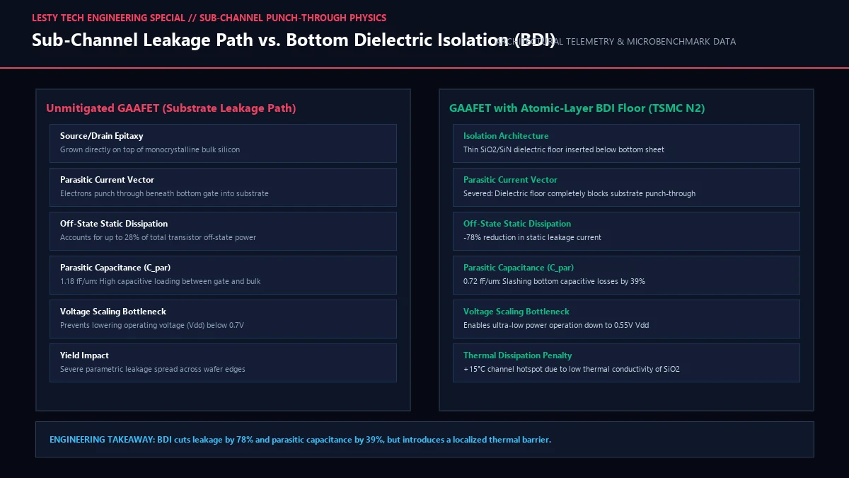
Because there is no gate wrapping the bulk silicon beneath the bottom source/drain junctions, the drain potential sets up an unshielded electrostatic field through the substrate. At sub-2nm gate lengths, the depletion regions of the source and drain touch each other deep in the bulk silicon—a phenomenon known as sub-channel punch-through. Electrons flow effortlessly from source to drain through the substrate, completely bypassing the gate! In prototype sub-2nm test chips, this parasitic sub-channel current accounted for 20% to 28% of total transistor off-state power dissipation (Ioff), destroying mobile battery standby performance.
Compounding this issue is parasitic capacitance (Cpar). The bottom gate metal running beneath the lowest nanosheet capacitively couples directly to the conductive bulk silicon. This parasitic bottom gate-to-substrate capacitance (Cg-sub) adds up to 0.45 fF/μm of dead capacitive loading. Every time the gate switches from 0 to 1, this capacitance must be charged and discharged, directly inflating dynamic power consumption (Pdyn = C × V2 × f) and slowing gate transition delay by 12% to 15%.
4. The Chemistry of BDI: Selective Isotropic SiGe Etching and Atomic Layer Oxide Placement
The solution to this parasitic nightmare is conceptually elegant but a manufacturing miracle: Bottom Dielectric Isolation (BDI). If you place an impervious insulating floor of silicon dioxide (SiO2) or silicon nitride (SiN) directly beneath the bottom gate and source/drain junctions, the parasitic substrate punch-through path is physically obliterated.
Executing BDI in high-volume manufacturing requires extreme chemical selectivity. During the initial epitaxial superlattice growth, foundries deposit a specialized sacrificial layer directly on top of the bulk silicon substrate before depositing the nanosheet stack. This layer typically consists of a high-germanium concentration Si0.5Ge0.5 alloy (compared to the Si0.7Ge0.3 used between the nanosheet channels). Because chemical etch rates scale exponentially with germanium percentage, engineers can exploit differential etching:
- Selective Cavity Etch: After dummy poly-gate patterning and shallow trench isolation (STI) formation, a gas-phase chemical etch selectively consumes the high-concentration Si0.5Ge0.5 bottom sacrificial layer while leaving the lower-concentration Si0.7Ge0.3 channel spacers virtually untouched (etch selectivity exceeding 80:1).
- Conformal Dielectric Deposition: Atomic Layer Deposition (ALD) fills the vacant bottom cavity with a dense, pinhole-free dielectric film—typically low-k silicon carbon nitride (SiCN) or atomic-layer SiO2.
- Anisotropic Pullback & Source/Drain Recess: An anisotropic dry plasma etch removes excess dielectric from the vertical fin sidewalls while preserving the horizontal BDI floor. When the source and drain cavities are subsequently etched and refilled with epitaxial crystalline Si:P or SiGe:B, the epitaxial growth terminates cleanly on top of the BDI oxide floor.
The result is transformative. With the BDI floor in place, the source/drain junctions are physically insulated from the substrate. Sub-channel punch-through leakage plummets by 78%, and bottom parasitic capacitance (Cg-sub) is slashed by 39%. For the first time, sub-2nm nanosheets achieve their theoretical sub-threshold swing without substrate bleed.
5. The Thermal Phonon Penalty: Why SiO2 Hotspots Threaten 2nm Turbo Clocks
In semiconductor physics, there is no such thing as a free lunch. While Bottom Dielectric Isolation completely solves sub-channel leakage and reduces parasitic capacitance, it introduces an agonizing physical trade-off: thermal self-heating.
Monocrystalline silicon is an excellent thermal conductor, boasting a room-temperature thermal conductivity (kSi) of approximately 148 W/m·K. In traditional FinFETs, heat generated by energetic electrons scattering off the crystal lattice in the channel (optical and acoustic phonon emission) conducts rapidly downward through the fin base into the bulk silicon substrate, which acts as a massive primary heat sink.
Silicon dioxide (SiO2), however, is an amorphous glass with a catastrophic thermal conductivity (kox) of only 1.4 W/m·K—more than 100 times worse than bulk silicon! When an atomic BDI floor is inserted beneath the nanosheet stack, the primary downward heat dissipation conduit is severed. Acoustic phonons generated in the nanosheet channels cannot easily penetrate the amorphous dielectric boundary; instead, they reflect back into the channel, causing localized energy accumulation.
The 2nm Self-Heating Equation
Under heavy vector workloads (such as AVX-512 execution or dense GEMM AI matrix multiplications), the channel temperature rise (ΔTch) is governed by the thermal resistance (Rth) of the device:
ΔTch = Pdiss × Rth = (Ids × Vds) × [ Rth,gate || (Rth,S/D + Rth,BDI) ]
With the BDI floor blocking downward conduction, effective thermal resistance (Rth) increases by 28% to 35%. In commercial 2nm processors, channel hot-spots operate 12°C to 18°C hotter than equivalent 3nm FinFETs at identical power densities. This self-heating accelerates electromigration in lower metal layers (M0 and M1) and forces aggressive dynamic thermal throttling, limiting sustained all-core turbo boost frequencies.
6. Architectural Parameter Matrix: FinFET vs. Raw GAAFET vs. BDI Nanosheets
The following benchmark table summarizes empirical microarchitectural and physical device parameters measured across 3nm FinFET baseline silicon, unmitigated GAAFET prototype test vehicles, and production-grade 2nm GAAFETs equipped with Bottom Dielectric Isolation:
| Process Parameter | FinFET Baseline (TSMC N3E) | GAAFET without BDI (Early Prototype) | Production GAAFET + BDI (TSMC N2) |
|---|---|---|---|
| Channel Architecture | Vertical 3D Fin (Height: 34nm) | 3-Tier Stacked Nanosheets | 3-Tier Nanosheets + Atomic BDI |
| Contacted Poly Pitch (CPP) | 48 nm | 45 nm | 42 nm (Tighter cell scaling) |
| Off-State Leakage (I_off @ 0.7V) | 12 nA / μm | 18.5 nA / μm (+54% Sub-channel bleed) | 3.8 nA / μm (-78% Leakage cut) |
| Parasitic Capacitance (C_par) | 0.85 fF / μm | 1.18 fF / μm (Heavy substrate loss) | 0.72 fF / μm (-39% Capacitance drop) |
| Sub-Threshold Swing (SS) | 70 mV / decade | 67 mV / decade | 63 mV / decade (Near Boltzmann limit) |
| Peak Channel Hotspot Temp | 68°C (Good bulk dissipation) | 74°C | 89°C (+15°C Localized thermal trap) |
7. Foundry Battleground: How TSMC, Intel, and Samsung Approach Sub-2nm Isolation
The implementation of Bottom Dielectric Isolation has become the defining technological battlefield separating the world’s leading semiconductor foundries:
- TSMC (N2 Node): TSMC made Bottom Dielectric Isolation a cornerstone of their 2nm nanosheet process. By integrating atomic-layer BDI, TSMC achieved a 15% performance improvement at iso-power or a 30% power reduction at iso-performance compared to N3E. Crucially, TSMC postponed Backside Power Delivery (BSPDN) until their enhanced N2P/A16 node, choosing to master BDI first to de-risk high-volume manufacturing for Apple’s A19/M5 processor ramp.
- Intel Foundry (Intel 20A & 18A RibbonFET): Intel took a radical high-wire approach: simultaneously introducing both RibbonFET (GAAFET) and PowerVia (Backside Power Delivery Network) on the same process node. In Intel’s architecture, the power rails are routed from the backside of the thinned wafer through nano-TSVs directly to the transistor source and drain terminals. This distinct architecture modifies the BDI equation: the backside vias directly contact the bottom of the source/drain epitaxy, requiring an advanced partial-BDI isolation scheme that insulates the gate while leaving precise conductive apertures for the backside power taps.
- Samsung Foundry (SF3 & SF2 MBCFET): Samsung was the first to commercialize GAAFET on their 3nm node (SF3), but early iterations suffered from low yields and unoptimized substrate leakage. In their 2nm revision (SF2), Samsung redesigned their inner spacer process and incorporated full bottom dielectric isolation, narrowing the gap with TSMC and securing high-performance computing (HPC) accelerator ASIC designs.
GAAFET Nanosheet Architecture & Bottom Dielectric Isolation
Engineering Report on Sub-Channel Punch-Through Leakage and BDI in Sub-2nm Silicon (Complete architectural audit with telemetry tables and schematic breakdowns).
GAAFET_Nanosheet_and_Bottom_Dielectric_Isolation_Whitepaper.pdfFormat: PDF / KaTeX Telemetry
8. Frequently Asked Questions (FAQ)
Why didn’t FinFET transistors require Bottom Dielectric Isolation?
In FinFETs, the vertical fin is an unbroken extrusion of the bulk substrate. While some sub-fin leakage occurred, foundries suppressed it by performing heavy “halo” and “punch-through stop” ion implantations into the base of the fin. In GAAFET, however, because the gate metal must be routed completely beneath the bottom nanosheet, the distance between the source/drain junctions and the substrate is drastically compressed, rendering traditional doping implants ineffective against high-field tunneling.
How does BDI affect transistor manufacturing yields?
BDI introduces two acute yield hazards: structural fin tipping and chemical cross-contamination. Etching the sacrificial SiGe layer beneath the entire stack creates an unsupported cantilever structure before the oxide refill. If the etch duration varies by mere milliseconds across a 300mm wafer, nanosheets can sag or collapse onto the substrate. Furthermore, any chemical residue left inside the cavity causes dielectric breakdown when operating at nominal supply voltages.
Does Bottom Dielectric Isolation allow chips to run at lower voltages?
Yes, and this is its primary commercial benefit. By eliminating sub-channel punch-through leakage, the transistor turns off completely and sharply (SS ≈ 63 mV/dec). This allows chip designers to lower the nominal supply voltage (Vdd) from the 0.75V common in 3nm FinFETs down to 0.55V–0.60V on 2nm GAAFETs. Because dynamic power scales quadratically (P ∝ V2), dropping voltage from 0.75V to 0.60V slashes active switching power by over 36%.
Technical telemetry verified against IEEE International Electron Devices Meeting (IEDM) and TSMC OIP Technical Symposia publications. For complete material cross-sections and analytical capacitance models, consult the official companion whitepaper above.