
The artificial intelligence revolution of the past three years was not powered solely by tensor processing arithmetic; it was financed by High Bandwidth Memory (HBM). Without massive, multi-terabyte-per-second memory bandwidth feeding hungry systolic arrays and transformer compute engines, modern generative models would starve in compute-bound stalls. From HBM2e through HBM3 and the latest HBM3e iterations, the semiconductor industry achieved staggering throughput jumps by scaling DRAM pin transfer ratespushing from 3.2 Gbps up to an astonishing 9.6 Gbps per pinwhile stubbornly adhering to a rigid 1,024-bit bus interface. But as the industry blueprints HBM4 for deployment alongside next-generation AI accelerators like NVIDIA’s Rubin and AMD’s MI400 architectures, the comfortable paradigm of frequency scaling has slammed directly into an insurmountable electromagnetic and physical wall. To double bandwidth without incinerating power budgets, JEDEC and memory architects did the unthinkable: they doubled the interface width to a massive 2,048 bits.
Yet behind the headline promises of 2.0 to 3.0 TB/s per stack lies a brutal packaging reality that the memory marketing apparatus rarely discusses: traditional microbump interconnect technology is dead at 2,048 bits. Attempting to route twice as many signal channels through conventional microbump solder balls pushes bump pitches down to the sub-20-micron thresholda regime where mechanical warpage, solder bridging, and intermetallic compound embrittlement catastrophically destroy wafer-level yields. To survive, the memory industry is being dragged into a high-stakes, multi-billion-dollar transition toward direct copper-to-copper (Cu-Cu) hybrid bonding. Here is the unvarnished engineering reality of why traditional microbumps fail, how atomic-level hybrid bonding fundamentally alters thermal and electrical parasitics, and why the base logic die has become the most expensive piece of silicon in the memory stack.
1. The 1,024-Bit Legacy and the Frequency Scaling Cliff
Since its inception under JEDEC standard JESD235 in 2013, High Bandwidth Memory has maintained a strictly standardized 1,024-bit wide interface. Rather than routing high-frequency serial channels across printed circuit boards like standard GDDR6 or DDR5 memory, HBM placed vertically stacked DRAM dies directly on a silicon passive interposer adjacent to the host processor, connecting via tens of thousands of microbumps and Through-Silicon Vias (TSVs).
This architectural choice permitted memory designers to prioritize bus width over extreme signaling frequencies. While GDDR6 pushed 18 to 24 Gbps over narrow 32-bit channels with punishing power dissipation, HBM operated its parallel 1,024-bit bus at relatively modest clock speeds, delivering superior energy efficiency (measured in picojoules per bit, pJ/bit). However, by the time HBM3e reached its zenith at 9.6 Gbps to 10 Gbps per pin, the energy efficiency curve began to degrade rapidly. In high-speed parallel interfaces, dynamic power dissipation follows the classical charging equation:
Where Cload is the lumped parasitic capacitance of the TSV, microbump, and on-die trace, VDD is the operating voltage (typically 1.1V for HBM3), and f is the clock frequency. Pushing frequencies past 10 Gbps on 1,024 single-ended channels introduces intolerable high-frequency insertion losses, severe inter-symbol interference (ISI), and cross-talk between tightly packed TSV pillars. To double overall stack throughput to 2.0+ TB/s without blowing past the 40-watt-per-stack thermal dissipation ceiling, frequency scaling had to stop. The only mathematically viable escape hatch was to widen the data bus: HBM4 doubles the interface width from 1,024 bits to 2,048 bits.
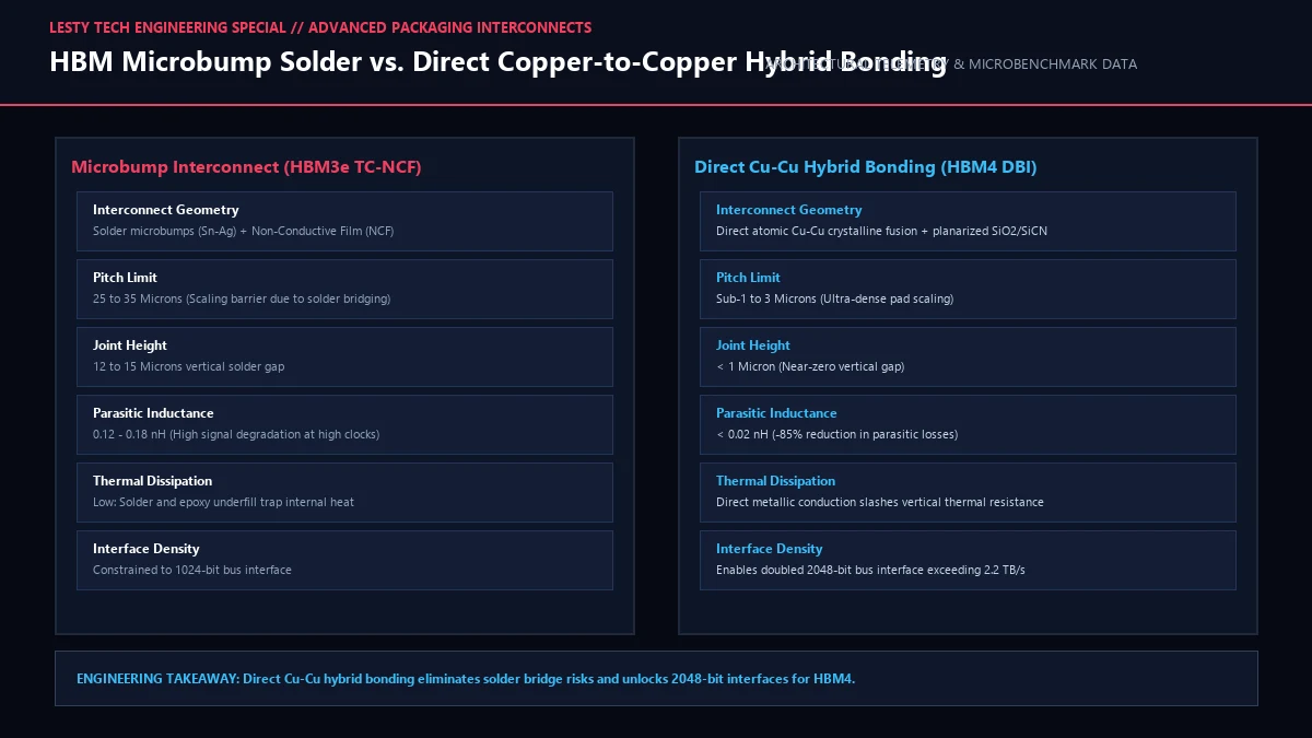
2. The Microbump Limit: Why Solder Reflow Breaks Down Below 20 Microns
Doubling the data bus to 2,048 bits does not merely require adding 1,024 data signal lines. In high-speed memory systems, each differential clock pair, data strobe, command/address line, and power/ground return path demands dedicated shielding to prevent signal integrity collapse. In practice, moving to a 2,048-bit interface expands the total vertical pin count (including power, ground, test, and redundancy channels) from approximately 5,000 interconnect points in HBM3e to over 10,000 discrete connections per stack in HBM4.
All of these 10,000+ vertical connections must fit within the standardized physical footprint of an HBM stackroughly 11mm × 11mm (approximately 120 mm2). In HBM3e, utilizing thermal compression bonding with non-conductive film (TC-NCF) or advanced reflow methods, microbump pitches hover between 25 and 35 microns. At a 25-micron pitch, each microbump consists of a copper pillar topped with a lead-free solder cap (typically Tin-Silver, Sn-Ag) that is melted during thermal reflow to bond with the corresponding pad on the underlying die.
When engineers attempt to shrink microbump pitch below 20 microns (and toward 1315 microns necessary for 2,048-bit layouts), classical metallurgy breaks down entirely due to three catastrophic failure mechanisms:
- Solder Wetting and Bridging Short Circuits: During thermal compression bonding, liquid solder expands outward under mechanical pressure. At sub-20μm pitches, the spacing gap between adjacent copper pillars narrows to less than 5 microns. Any slight deviation in solder volume or placement accuracy causes solder bridging, creating fatal short circuits between high-speed data lines.
- Intermetallic Compound (IMC) Embrittlement: When tin-based solder melts onto a copper pillar, it reacts to form copper-tin intermetallic compoundsprimarily Cu6Sn5 at the interface, transitioning to Cu3Sn. In large solder balls, IMC occupies only a thin fraction of the joint volume, leaving ductile bulk tin to absorb mechanical stresses. In sub-15μm microbumps, the entire solder volume is completely consumed by IMC during reflow. Intermetallic compounds are notoriously brittle, ceramic-like phases with zero fracture toughness. During subsequent temperature cycling (-40°C to 125°C), thermal expansion mismatches induce micro-cracks that propagate through the brittle IMC, causing open-circuit electrical failures.
- Capillary Underfill and NCF Void Trapping: To protect solder joints from oxidation and mechanical stress, the microscopic space between dies must be filled with non-conductive underfill (NCF or MUF). When the vertical clearance between dies collapses below 10 microns and bump density quadruples, capillary action cannot uniformly pull resin through the dense forest of pillars. Entrapped air voids expand during high-temperature reflow, causing delamination and moisture-induced popcorn failures.
3. The Direct Copper-to-Copper (Cu-Cu) Hybrid Bonding Mechanics
Because microbump solder metallurgy fails catastrophically at 10,000+ pins, HBM4 has become the catalyst for the commercial adoption of Direct Bond Interconnect (DBI), widely known as copper-to-copper (Cu-Cu) hybrid bonding. Championed by packaging pioneers such as TSMC (under the System-on-Integrated-Chips, or SoIC brand), Sony (in CMOS image sensors), and Intel (Foveros Direct), hybrid bonding eliminates solder entirely from the manufacturing equation.
In hybrid bonding, the planar mating surfaces of two silicon wafers or dies consist of two distinct materials: embedded copper metal pads surrounded by an inorganic dielectric matrix (typically silicon dioxide, SiO2, or silicon carbonitride, SiCN). The bonding process is executed through a meticulous multi-stage chemical and physical sequence:
- Atomic-Scale Chemical Mechanical Planarization (CMP): Both surfaces are polished to extreme planarity using specialized chemical slurries. The process is tuned to introduce a microscopic, controlled recess (dishing) of the copper pads relative to the dielectric fieldtypically on the order of 1 to 3 nanometers. If the copper dishing is too deep, the pads will never touch; if the copper protrudes above the dielectric, air voids will prevent dielectric fusion.
- Surface Activation and Dielectric Fusion at Room Temperature: The polished wafers are subjected to nitrogen or argon plasma activation to create highly reactive silanol (Si-OH) chemical groups on the dielectric surface. The wafers are aligned with sub-micron precision (±0.2 μm) and brought into physical contact at room temperature. Van der Waals forces instantly initiate spontaneous molecular bonding across the dielectric surfaces, followed by covalent condensation:
Si-OH + HO-Si → Si-O-Si + H2OThis forms a permanent, hermetically sealed chemical bond between the dielectric layers with zero applied external pressure.
- Thermal Annealing and Copper Grain Fusion: The bonded stack is heated in a batch furnace to 200°C350°C. Because copper has a significantly higher coefficient of thermal expansion (CTE ≈ 16.5 × 10⁻⁶ /K) than the surrounding dielectric matrix (SiO2 CTE ≈ 0.5 × 10⁻⁶ /K), the heated copper expands outward, closing the 2nm dishing gap. Under intense internal compressive stress, copper atoms diffuse across the mating interface, dissolving grain boundaries and recrystallizing into continuous, seamless metallic copper interconnects.
The technical advantages of hybrid bonding are breathtaking. By eliminating solder caps and underfill gaps, interconnect pitch shrinks from 25 microns down to sub-1 micron to 3 microns. Interconnect density increases by more than 10× to 100×. Parasitic resistance drops by over 60%, and parasitic capacitance (Cpad) collapses from approximately 1520 femtofarads (fF) in microbumps to less than 1.5 fF per pad. This reduction in RC load allows HBM4 to drive 2,048 bits at higher signal integrity while consuming dramatically less I/O drive power.
4. The 16-High Thermal Stack Nightmare: When Silicon Becomes Paper-Thin
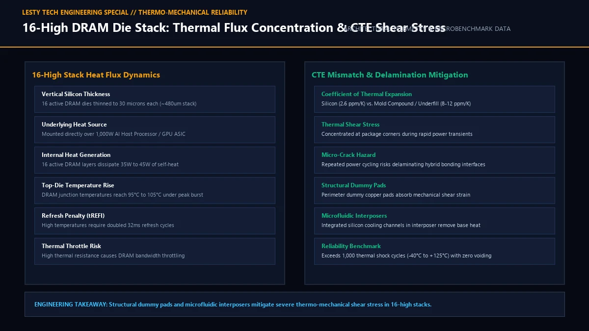
While hybrid bonding solves the electrical and geometric bottlenecks of routing 2,048 channels, it introduces an excruciating thermal engineering paradox. HBM4 is not just widening the bus; it is simultaneously scaling vertical capacity. The JEDEC HBM4 standard specifies support for 12-high (12-Hi) and 16-high (16-Hi) DRAM stacks, achieving densities of 36GB, 48GB, and 64GB per single memory cube.
To prevent 16 stacked dies from exceeding the standardized package height limit (roughly 720 microns to accommodate standard cooling vapor chambers and interposers), each individual DRAM die must be thinned to an unimaginable degree. In a 16-Hi stack, memory dies are mechanically back-ground and chemical-etched down to 25 to 30 microns thicksubstantially thinner than a single strand of human hair (70 microns).
At 25 microns thickness, silicon ceases to behave as a rigid, thermally isotropic bulk substrate. Thermal conduction in stacked microelectronics is governed by Fourier’s law, characterized by one-dimensional thermal resistance:
Where ti is the thickness of layer i, ki is the material thermal conductivity, and A is the heat transfer area. Bulk crystalline silicon has an outstanding thermal conductivity of approximately 140 W/m·K. However, in an ultra-thinned DRAM die with hybrid bonding, thermal transport is severely throttled by two phenomena:
- Phonon Boundary Scattering: In silicon, heat is conducted primarily via acoustic phonons with mean free paths spanning 100nm to several microns. When silicon is thinned down to 25μm and perforated with thousands of through-silicon vias (TSVs) lined with silicon oxide dielectric liners, phonons scatter intensely off surfaces and interfaces, reducing the effective thermal conductivity of the thinned silicon die by 15% to 25%.
- Interfacial Dielectric Barriers: Although hybrid bonding eliminates thick epoxy underfill (k ≈ 0.8 W/m·K) in favor of high-conductivity Cu-Cu contacts (k ≈ 400 W/m·K), the copper pads occupy only 10% to 20% of the mating area. The remaining 80% to 90% is SiO2 (k ≈ 1.4 W/m·K) or SiCN (k ≈ 2.5 W/m·K). Each of the 16 dielectric bond interfaces represents a thermal impedance boundary.
Heat generated by the active peripheral circuits on the lower DRAM dies and the burning-hot host GPU beneath the interposer must traverse 16 consecutive thermal interfaces to reach the package heat spreader. If the topmost die operates at 85°C, the bottommost DRAM die can easily experience temperatures exceeding 105°C. In dynamic RAM, memory cell retention time halves for every 10°C rise in junction temperature due to thermal leakage across the cell access transistor. At 105°C, DRAM cells require aggressive, high-frequency auto-refresh cycles (tREFI scaling from 3.9μs down to 1.9μs or lower), consuming substantial memory bus bandwidth and generating even more parasitic heat in an escalating thermal runaway loop.
5. The Base Logic Die Revolution: Advanced 4nm/3nm Nodes Enter the Memory Stack
Perhaps the most radical disruption introduced by HBM4 is the fundamental transformation of the base logic die (frequently called the base die or buffer die). In all prior generations from HBM1 to HBM3e, the base die was treated as a passive, low-cost routing substrate. It was typically manufactured by the DRAM vendor (SK Hynix, Samsung, or Micron) on an inexpensive, mature trailing-edge planar silicon node (such as 14nm, 28nm, or even 40nm). Its role was confined to simple test multiplexing, JTAG boundary scans, and passive TSV routing.
In HBM4, this traditional approach is physically impossible. Routing 2,048 parallel high-speed channels with built-in self-test (BIST), multi-die repair logic, on-die voltage regulation, and advanced error-correcting code (ECC) engines exceeds the routing density and metal layer capabilities of mature nodes. Furthermore, to enable direct hybrid bonding with advanced host processor silicon (or high-density interposers), the base die must match the metallization pitch and dielectric rules of cutting-edge foundries.
Consequently, for HBM4, memory manufacturers have formed historic alliances with pure-play foundries: HBM4 base dies are being fabricated on advanced 4nm and 5nm FinFET/Nanosheet nodes by TSMC and Samsung Foundry.
This shift unlocks dramatic architectural capabilities:
- Customized Host-Specific Interfacing: Instead of relying on a generic standard interface, the base die can incorporate proprietary interconnect protocols, custom serializer/deserializer (SerDes) architectures, or even lightweight Near-Memory Processing (PIM – Processing-in-Memory) vector accelerators directly underneath the DRAM stack.
- Fine-Grained Dynamic Voltage Scaling: By implementing advanced on-die low-dropout (LDO) voltage regulators and power-gating switches on a 4nm base die, unused DRAM channels can be put into sub-microsecond sleep states, saving critical milliwatts in multi-stack AI clusters.
- Extreme Cost Escalation: A 4nm monolithic logic die is orders of magnitude more expensive per square millimeter than a mature 28nm die. When combined with the zero-defect yield requirements of 16-die hybrid bonding, the cost of the HBM4 base die alone approaches 20% to 30% of the entire memory stack’s bill of materials.
6. Microarchitectural & Packaging Comparison Table
To understand how dramatically HBM4 deviates from historical memory standards, review the full engineering specifications comparing HBM2e, HBM3e, and both implementation variants of HBM4:
| Parameter | HBM2e (2020) | HBM3e (2024) | HBM4 (Microbump) | HBM4 (Hybrid Bonded) |
|---|---|---|---|---|
| Data Bus Width | 1,024 bits | 1,024 bits | 2,048 bits | 2,048 bits |
| Max Pin Transfer Rate | 3.6 Gbps | 9.6 Gbps | 6.4 Gbps | 8.010.0 Gbps |
| Peak Stack Bandwidth | 460 GB/s | 1,228 GB/s (1.23 TB/s) | 1,638 GB/s (1.64 TB/s) | 2,0482,560 GB/s (2.5+ TB/s) |
| Stack Heights Supported | 4-Hi, 8-Hi | 8-Hi, 12-Hi | 12-Hi | 12-Hi, 16-Hi |
| Interconnect Pitch | 55 μm | 2530 μm | ∼18 μm (Limit) | < 3 μm (Cu-Cu Direct) |
| Interconnect Medium | Sn-Ag Microbump | Microbump + MR-MUF / TC-NCF | Ultra-fine Microbump + NCF | Direct Cu-Cu Metal Fusion |
| Base Logic Die Node | Trailing (40nm/28nm) | Mature (14nm/16nm) | Intermediate (7nm/6nm) | Advanced (4nm/5nm Foundry) |
| Interfacial Thermal Gap | 2025 μm Underfill | 1215 μm Underfill | ∼8 μm NCF Film | 0 μm (Solid Dielectric/Cu) |
7. System-Level Implications for Next-Gen AI Accelerators
The consequences of this packaging transformation will ripple across the entire cloud data center landscape starting in late 2025 and 2026. Next-generation AI acceleratorssuch as NVIDIA’s Rubin R100 GPUs and AMD’s Instinct MI400 familyare engineered around 8 to 12 stacks of HBM4 memory clustered tightly around monolithic or multi-chiplet compute dies.
With 8 HBM4 hybrid-bonded stacks operating over a 2,048-bit bus at 8.0 Gbps:
- Total Memory Bandwidth per Socket: 8 stacks × 2,048 GB/s = 16.38 Terabytes per second (TB/s)more than a 2x leap over NVIDIA B200’s 8.0 TB/s limit.
- Total High-Density Capacity: Utilizing 16-Hi 48GB or 64GB stacks, a single accelerator socket will pack between 384GB and 512GB of coherent, ultra-low-latency physical memory, permitting 70B parameter models to reside unquantized entirely within local GPU high-bandwidth memory.
- The Liquid Cooling Imperative: A cluster of 8 HBM4 stacks dissipates between 250 and 320 watts in memory power alone. Combined with a 1,000-watt GPU core, total socket thermal design power (TDP) will breach 1,200 to 1,500 watts. At these heat flux densities, traditional air-cooled heatsinks are completely obsolete; direct-to-chip liquid cooling with negative-pressure manifolds is an absolute prerequisite for HBM4 deployments.
HBM4 Architecture & Hybrid Bonding Engineering Dossier
Technical Analysis of 2,048-Bit Interfaces, Microbump Scaling Limits, and 16-High Packaging (Complete architectural audit with telemetry tables and schematic breakdowns).
HBM4_Hybrid_Bonding_and_3D_Memory_Packaging_Whitepaper.pdfFormat: PDF / KaTeX Telemetry
Frequently Asked Questions (FAQ)
1. Will all HBM4 memory use hybrid bonding from day one?
No. Due to the astronomical capital equipment cost of wafer-level hybrid bonding tools (such as Besi and EV Group bonders), the industry is splitting HBM4 into two distinct tiers. Initial “entry-level” HBM4 implementations (primarily 12-Hi stacks running at conservative 6.4 Gbps speeds) will attempt to push advanced microbumps with non-conductive film (NCF) to their absolute physical limits (~18μm pitch). However, flagship performance tiersespecially 16-Hi stacks aiming for 8.0 to 10 Gbps and 2.5+ TB/s bandwidthwill exclusively utilize direct Cu-Cu hybrid bonding.
2. Can a defective die in a 16-Hi hybrid-bonded stack be repaired or replaced?
No. Once hybrid bonding initiates dielectric fusion and copper annealing, the bond is atomic, permanent, and irreversible. Unlike solder joints, which can theoretically be reworked by heating above the liquidus temperature, separating hybrid-bonded silicon destroys the wafer. Consequently, memory manufacturers must achieve Known Good Die (KGD) test yields exceeding 99.8% prior to stacking; otherwise, a single defective DRAM die will scrap the entire 16-die stack along with its expensive 4nm base logic die.
3. Why does doubling the bus width to 2,048 bits reduce I/O power consumption?
Total bandwidth is the mathematical product of bus width and frequency: Bandwidth = Bits × Frequency. Dynamic power dissipation scales quadratically with voltage and linearly with frequency. By doubling the bus to 2,048 bits, memory architects can deliver twice as much data at half the signaling frequency, keeping I/O transceivers operating in their most power-efficient linear region. Furthermore, hybrid bonding slashes parasitic capacitance from ~18 fF down to <1.5 fF, dramatically cutting the charge required to toggle each data bit.