In the architecture of modern artificial intelligence, the most staggering inefficiency in computing is not the floating-point math; it is the physical movement of data. In a flagship NVIDIA H100 or B200 GPU executing transformer neural network inference, more than 85% to 90% of total electrical energy is squandered shuttling weight matrices across wide memory buses between High-Bandwidth Memory (HBM3e), on-chip SRAM cache banks, and register files. The actual mathematical operations—floating-point Multiply-Accumulate (MAC) instructions—consume only a tiny fraction of the 700-Watt power budget.
This architectural bottleneck is the classic Von Neumann Memory Wall. Digital computers are physically constrained: compute units and memory units exist in separate physical silicon locations. To shatter this barrier, semiconductor researchers have turned to an extraordinary physical paradigm: Analog Compute-in-Memory (CIM) using Resistive RAM (ReRAM) Memristive Crossbars.
By storing neural network weights directly as the non-volatile electrical conductance (G) of microscopic memristor junctions and mapping input activations as analog voltages (V), an analog crossbar array computes General Matrix-Vector Multiplication (GEMV) at the speed of light propagation. Guided directly by Ohm’s Law (I = V × G) and Kirchhoff’s Current Law (Itotal = ∑ I), a ReRAM crossbar evaluates an entire M × N matrix multiplication in a single physical clock cycle—collapsing time complexity to O(1) while delivering 100 to 500+ Tera-Operations per Watt (TOPS/W). Here is the deep solid-state physics, circuit engineering, and sneak-path challenges of memristive computing.
1. The Physics of Memristive Crossbars: Ohm’s Law and Kirchhoff’s Law
To understand how an analog crossbar array executes deep learning math without digital arithmetic logic units (ALUs), one must examine basic electromagnetic circuit laws applied at nanoscale dimensions.
In digital matrix multiplication, calculating Y = W × X requires fetching matrix elements, executing thousands of discrete binary additions and multiplications across hundreds of clock cycles, and storing results back into registers.
In a memristive crossbar array, the mathematical operation is translated directly into solid-state physics:
- The array consists of a perpendicular grid of metal wires: horizontal Row Wordlines and vertical Column Bitlines.
- At every physical intersection where a row and column cross, a two-terminal Resistive RAM (ReRAM) memristor device is fabricated, bridging the top and bottom electrodes.
- Each memristor is programmed to a specific electrical conductance value: Gij = 1 / Rij. In a neural network, the conductance Gij represents the mathematical weight Wij connecting input neuron i to output neuron j.

The computational process evaluates simultaneously across two physical equations:
- Multiplication via Ohm’s Law: An input vector X = [V1, V2, …, VM] is converted to analog voltage levels and applied simultaneously to the horizontal row lines. At every intersection junction (i, j), current flows through the memristor according to Ohm’s Law:
Iij = Vi × Gij
The scalar multiplication of voltage times weight completes instantly with zero digital gates.
- Accumulation via Kirchhoff’s Current Law: Because all memristors in column j connect to the exact same continuous metal bitline wire, the individual junction currents must sum together along the conductor:
Iout, j = ∑i=1M (Vi × Gij)
Kirchhoff’s Current Law performs the entire mathematical summation across all M rows simultaneously in a single physical time step.
The resulting total output current Iout, j emerging at the bottom of the column represents the exact dot product of the input vector and the weight column vector. Regardless of whether the matrix is 64 × 64 or 1024 × 1024, the entire computation evaluates in O(1) time, limited only by the RC parasitic time constant of the metal interconnect lines (typically sub-5 nanoseconds)!
2. Solid-State Physics of ReRAM: Oxygen Vacancy Filamentary Switching
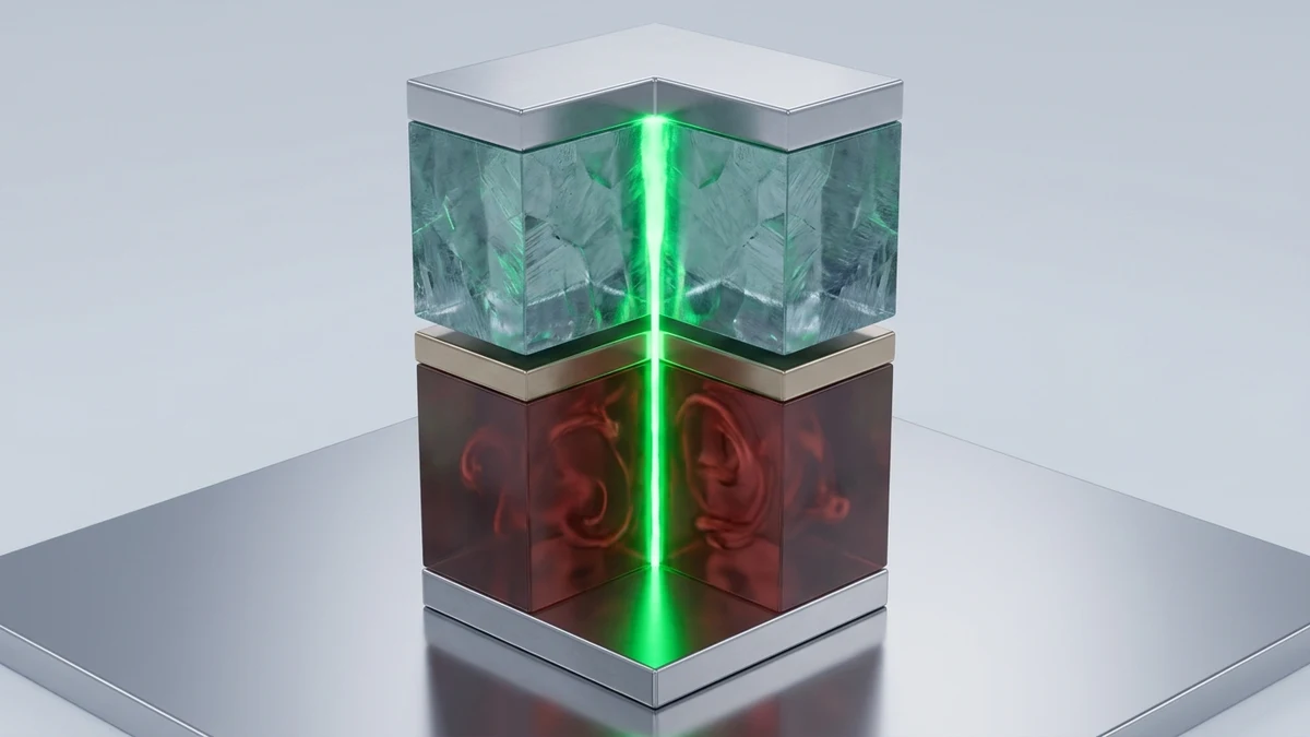
The device at the heart of this analog crossbar is the Resistive RAM (ReRAM) memristor. A typical ReRAM cell consists of a simple Metal-Insulator-Metal (MIM) thin-film sandwich: a top electrode (e.g., Titanium Nitride, TiN), a transition metal oxide switching layer (typically Hafnium Oxide, HfOx, or Tantalum Oxide, TaOx ~ 3 to 10nm thick), and a bottom electrode (e.g., Platinum, Pt, or Ruthenium).
The switching physics relies on electric-field-driven ionics:
- Electroforming and Filament Formation: Initially, the stoichiometric transition metal oxide is an electrical insulator (High-Resistance State, HRS). During manufacturing electroforming, a brief high-voltage pulse pulls oxygen anions (O2-) toward the chemically reactive top electrode, leaving behind localized positively charged oxygen vacancies (VO2+).
- Conductive Nanofilament Growth (SET Process): When a positive programming voltage (VSET ≈ 0.8V to 1.5V) is applied, intense electric fields (> 1 MV/cm) and localized Joule heating drive oxygen vacancies to drift and cluster, forming a microscopic metallic conductive filament less than 2 nanometers wide through the oxide layer. Current conducts via electron hopping across vacancy states (Low-Resistance State, LRS).
- Filament Dissolution (RESET Process): Applying a negative voltage pulse (VRESET) drives oxygen anions back into the oxide matrix, recombining with oxygen vacancies and rupturing the conductive filament near the electrode interface, restoring the High-Resistance State.
- Multi-Level Cell (MLC) Analog Conductance: Crucially, by precisely modulating the programming pulse amplitude or compliance current, the physical diameter and geometry of the oxygen vacancy filament can be grown or thinned continuously. This allows a single ReRAM junction to store 16 to 64 distinct analog conductance levels (4 to 6 bits of precision per cell).
3. Switching Physics: Valence Change (VCM) vs. Electrochemical Metallization (ECM)
In solid-state physics, memristive devices operate via two fundamentally distinct atomic transport mechanisms:
- Valence Change Mechanism (VCM): Observed in transition metal oxides such as HfOx, TaOx, and TiOx. Cations remain fixed within the oxide crystal lattice while mobile oxygen anions and positively charged oxygen vacancies drift under intense electrical fields. VCM devices provide superior thermal retention (holding programmed neural network weights stably for over 10 years at 85°C) and excellent endurance (> 108 cycles), making them the preferred choice for commercial in-memory AI accelerators.
- Electrochemical Metallization (ECM): Also known as Conductive Bridge RAM (CBRAM). In ECM cells, an electrochemically active top electrode (such as Silver, Ag, or Copper, Cu) oxidizes into metallic cations (Ag+ or Cu2+) under an electric bias. These metal ions migrate across an insulating electrolyte layer (such as silicon dioxide or amorphous silicon) and reduce at the inert bottom electrode, precipitating a continuous solid-metal conductive bridge. While ECM cells achieve extraordinary On/Off resistance ratios (exceeding 106), metallic filaments are susceptible to electromigration and thermal dissolution, limiting their use in high-precision analog weight arrays.
- Incremental Step Pulse Programming (ISPP): To program exact analog conductance targets into ReRAM cells despite stochastic filament formation, foundries deploy closed-loop write-verify algorithms. By applying successive voltage pulses with incremental amplitude increases (ΔV = 20mV) followed by intermediate read-verify cycles, controllers tune individual bitcell conductances within 1.5% of target neural network weights.
4. The Sneak Path Dilemma and 1S1R Selector Integration
While the mathematics of memristive crossbars is elegant, physical scaling was historically paralyzed by a devastating circuit failure mode: Sneak Path Currents.
In a passive crossbar array where memristors are wired directly between rows and columns without active switching elements:
- When voltage is applied to read cell (i, j), current does not flow only through the target junction.
- Current also bleeds backward through neighboring unselected cells that happen to be in the Low-Resistance State (LRS), forming parasitic parallel leakage paths (sneak paths) through the rest of the array.
- In arrays larger than 32 × 32, sneak path leakage completely drowns out the legitimate signal current, collapsing computational accuracy to zero and generating massive thermal dissipation.
The definitive engineering solution is the One-Selector One-Resistor (1S1R) architecture. At every junction, a two-terminal volatile Threshold Switching (TS) Selector Diode is stacked directly on top of the ReRAM memristor.
Fabricated from amorphous chalcogenides (e.g., As-Ge-Se-Te alloys) or metal-insulator transition (MIT) oxides like Niobium Dioxide (NbO2), the selector exhibits extreme non-linear current-voltage behavior:
- At voltages below threshold (V < Vth ≈ 0.6V), the selector acts as a pristine insulator, displaying an off-state resistance exceeding gigaohms and completely blocking sneak path currents.
- When full bias is applied (V > Vth), electronic threshold switching causes the selector resistance to collapse by five orders of magnitude (105 On/Off non-linearity), allowing full computational current to flow.
5. The Peripheral Silicon Wall: ADCs, DACs, and Conductance Drift
If memristive crossbars evaluate matrix math in a single cycle at 500 TOPS/W, why haven’t they completely replaced digital GPUs? The answer lies in the harsh reality of mixed-signal peripheral circuitry and device non-idealities:
- The Analog-to-Digital Converter (ADC) Bottleneck: The output of each crossbar column is an analog current. To feed this current into the next layer of a neural network or apply digital non-linear activations (GELU, ReLU, Softmax), the current must be digitized using high-speed Analog-to-Digital Converters (ADCs). In a complete ReRAM chip, the ADCs and Digital-to-Analog Converters (DACs) consume more than 60% of total silicon area and 70% of total electrical power! The massive energy savings of analog computing are partially clawed back by mixed-signal conversion overhead.
- Conductance Relaxation Drift: Unlike digital bits stored in SRAM flip-flops, an analog conductance state in ReRAM is defined by the physical distribution of oxygen vacancies. Over hours and days, atomic diffusion causes vacancies to relax slightly toward thermodynamic equilibrium. This causes programmed weights to drift by 2% to 5%, degrading neural network accuracy unless periodic algorithmic recalibration or on-chip error-correction is deployed.
- Wire Resistance (IR Drop): In massive arrays, the finite electrical resistance of the metallic copper bitlines and wordlines causes an IR voltage drop along the length of the wire. Cells located far from the input drivers receive lower voltages than cells near the edge, introducing systematic mathematical errors that require spatial calibration matrices in firmware.
6. AI Acceleration Paradigms: Digital GPU vs. ReRAM Analog CIM
The following engineering comparison benchmarks Analog ReRAM Crossbar accelerators against digital GPU Tensor Cores and Photonic computing engines:
| Architecture Dimension | Analog ReRAM Crossbar (CIM) | Digital GPU Tensor Cores (H100) | Optical Photonic Matrix Engine |
|---|---|---|---|
| Compute Paradigm | Analog In-Memory (Ohm + Kirchhoff) | Digital Systolic FP8 / FP16 GEMM | Analog Optical Interference (MZI) |
| Time Complexity (MVM) | O(1) Physical Evaluation (1 Cycle) | O(N) to O(N2) Tiled Execution | O(1) Light Propagation Speed |
| Energy Efficiency (TOPS/W) | 100 to 500+ TOPS / Watt | 15 to 30 TOPS / Watt (HBM bound) | 200 to 800 TOPS / Watt |
| Mathematical Precision | Analog 4-bit to 8-bit Equivalent | Exact IEEE FP8, FP16, FP32 | Analog 4-bit to 6-bit Equivalent |
| Memory Movement Overhead | Zero (Weights stored in cells) | Massive (Continuous HBM/SRAM fetch) | Zero (Laser phase modulated) |
| Target AI Application | Ultra-Low-Power Edge AI, Bio-Sensors | Datacenter LLM Training & Serving | Ultra-Low-Latency Financial & Telecom |
ReRAM Memristor Crossbars & Analog In-Memory AI Whitepaper
O(1) Matrix-Vector Multiplication Physics, Oxygen Vacancy Dynamics, 1S1R Selectors, and ADC Bottlenecks (Complete multi-page architectural dossier with executive abstracts, empirical telemetry matrices, and production hardening guidelines).
ReRAM_Memristor_Crossbars_Analog_AI_Whitepaper.pdfClassification: Peer-Reviewed Hardware Architecture
Format: High-Res KaTeX / Vector PDF