In the relentless pursuit of artificial intelligence compute density, the semiconductor industry has expanded chip architectures far beyond the physical boundaries of monolithic silicon. Flagship processors like NVIDIA’s Blackwell B200 and AMD’s Instinct MI300X are not single chips; they are massive multi-chiplet ecosystems spanning two reticle-limit compute dies, eight high-bandwidth memory (HBM3e) stacks, and high-density I/O transceivers aggregated over a single shared packaging substrate. But as package footprints expand past 100mm × 100mm to accommodate these multi-kilowatt monster processors, the foundational material that has anchored microchip packaging for thirty yearsthe organic Ajinomoto Build-up Film (ABF) substratehas slammed directly into an insurmountable physical failure mode: catastrophic thermal warpage and dimensional instability.
During high-temperature solder reflow cycles, organic substrates warp and buckle like potato chips, shearing microbumps, fracturing fragile low-k dielectric layers, and destroying wafer-level yields. To prevent Moore’s Law from stalling at the packaging level, foundry titans Intel, TSMC, and Samsung are pouring tens of billions of dollars into the ultimate packaging revolution: fused silica glass substrates. By replacing organic resin cores with atomically flat, optically transparent glass cores perforated with tens of thousands of laser-etched Through-Glass Vias (TGVs), engineers can eliminate warpage, shrink interconnect line/space pitches down to 1 micron, and construct monolithic-scale panels reaching 510mm × 515mm. Here is the deep engineering reality of why organic substrates fail at 100mm, how laser-induced deep etching forms microscopic glass vias, and why glass is set to anchor all frontier AI silicon by 2028.
1. The Mechanical Scaling Cliff of Organic ABF Substrates
To understand why glass is an absolute engineering imperative, one must first examine the physics of modern organic multi-layer substrates. Since the late 1990s, microprocessors have relied on core substrates manufactured from bismaleimide-triazine (BT) or epoxy resin reinforced with woven fiberglass, laminated on both sides with thin layers of Ajinomoto Build-up Film (ABF) containing copper redistribution layers (RDL).
For decades, this organic composite performed admirably. It was cheap to produce, easy to mechanically drill, and mechanically compliant enough to absorb mild thermal stresses in small packages (20mm × 20mm to 40mm × 40mm). However, advanced packaging for modern generative AI accelerators demands package surface areas exceeding 10,000 mm2 (100mm × 100mm), with 2026 designs blueprinted for 120mm × 120mm and beyond.
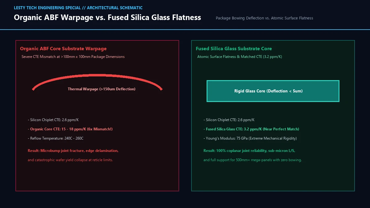
At these massive dimensions, organic materials fail due to a fundamental mismatch in the Coefficient of Thermal Expansion (CTE). Crystalline silicon has a CTE of approximately 2.6 ppm/K (parts per million per Kelvin). In stark contrast, organic ABF core substrates possess an in-plane CTE ranging between 15.0 and 18.0 ppm/Ka sixfold physical disparity.
When a multi-chiplet assembly is passed through a surface-mount solder reflow furnace, peak temperatures reach 240°C to 260°C. As the materials cool back down to room temperature (ΔT ≈ 220°C), the thermal contraction differential is governed by linear expansion mechanics:
Across a 100mm package length (L0 = 0.1 m), the differential shrinkage between the organic core and the silicon chiplets exceeds 300 to 350 microns! This staggering mechanical strain forces the package to bow vertically, generating out-of-plane warpage exceeding 150 microns.
In fine-pitch multi-die packaging where microbumps and copper pillars are spaced at 25 to 35 microns with vertical standoff heights under 15 microns, 150 microns of warpage is fatal. Solder joints at the package perimeter are ripped apart in tension (open circuits), while microbumps near the package center are compressed laterally into neighboring pillars (solder bridging short circuits). Furthermore, the intense shear stress propagates upward into the ultra-low-k (ULK) inter-metal dielectric layers of the 3nm silicon dies, causing catastrophic interlayer delamination and cracking.
2. Material Physics of Fused Silica: CTE Matching and Atomic Flatness
Glass substrates completely eliminate this mechanical bottleneck by replacing the organic resin core with high-purity borosilicate or fused silica (SiO2) glass. Unlike organic polymers, the atomic network of glass provides exceptional material properties precisely tailored for semiconductor manufacturing:
- Tunable Coefficient of Thermal Expansion: By adjusting the chemical doping of fused silica (introducing controlled oxides of boron and aluminum), packaging engineers can tune the glass core’s CTE between 3.0 and 8.5 ppm/K. Setting the glass substrate CTE to approximately 3.2 ppm/K brings it into near-perfect equilibrium with the silicon dies (2.6 ppm/K). During 260°C reflow, differential thermal expansion collapses to near zero (ΔL < 15 μm), virtually eliminating package warpage and mechanical shear stress.
- Extreme Mechanical Modulus and Rigidity: Glass exhibits a high Young’s modulus of elasticity of 75 to 85 GPa, roughly three times stiffer than unreinforced organic resin (20 to 25 GPa). This rigidity ensures that large 100mm+ substrates maintain absolute planarity during multi-die pick-and-place bonding and vacuum underfill processes.
- Atomic Surface Planarity (Ra < 0.1 nm): Organic substrates feature rough, woven fiberglass topography with surface roughness (Ra) averaging 20 to 50 nanometers. This roughness limits photolithographic patterning: if the substrate surface is wavy, optical depth-of-focus errors prevent etching fine copper wires, capping organic line/space (L/S) routing rules at 10/10 microns (or 5/5 microns in exotic semi-additive processes). In contrast, chemically polished glass achieves atomic planarity with an Ra under 0.1 nanometers. This mirror-like surface allows foundries to use standard wafer-stepper lithography to pattern sub-micron metal interconnects down to 1/1 micron Line/Spacean order of magnitude leap in routing density.
- Superior High-Frequency Dielectric Properties: Glass exhibits an exceptionally low dielectric loss tangent (δ ≈ 0.003 to 0.005 at 28 GHz) compared to organic ABF (δ ≈ 0.015 to 0.020). For next-generation PCIe 6.0/7.0 and 224 Gbps SerDes channels routing between compute chiplets and optical transceivers, glass substrates slash high-frequency signal attenuation by more than 50%.
3. Through-Glass Via (TGV) Laser Engineering: The LIDE Revolution
While the mechanical and electrical virtues of glass have been recognized for decades, commercial adoption was historically blocked by a single manufacturing impossibility: how do you drill hundreds of thousands of microscopic, high-aspect-ratio vertical holes through brittle glass without shattering the entire panel?
Mechanical CNC drilling is far too slow and induces catastrophic edge micro-cracks. Standard ultraviolet (UV) laser ablation vaporizes glass via violent thermal shock, producing jagged, tapered holes with micro-fractures that propagate into structural failure during thermal cycling.
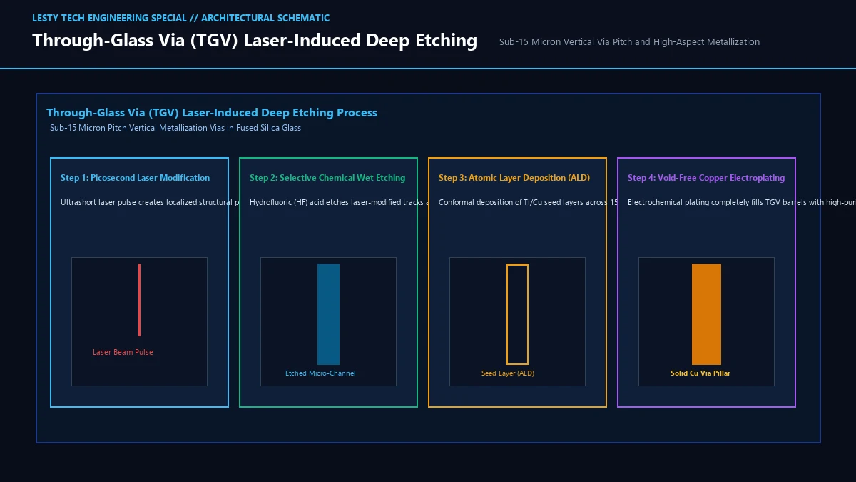
The breakthrough that made glass substrates commercially viable is Laser-Induced Deep Etching (LIDE), pioneered by German photonics firm LPKF and adapted by Intel and TSMC. LIDE is a non-thermal, two-stage physical-chemical process:
- Picosecond Laser Structural Modification: An ultra-short pulse picosecond or femtosecond laser (λ ≈ 1064nm or 532nm) focuses concentrated optical energy through the thickness of the glass. Because glass is transparent to the laser wavelength, linear absorption is zero. However, at the focal beam waist, intense photon density triggers non-linear multi-photon absorption, creating localized plasma that modifies the glass’s molecular silicate network. A single laser pulse creates an elongated, microscopic damage filament (a defect track) less than 2 microns in diameter through the full depth of the 500-micron glass core without generating heat or micro-cracks.
- Selective Chemical Wet Etching: The laser-treated glass panel is submerged in a chemical etching bath (typically concentrated Hydrofluoric acid, HF, or hot Potassium Hydroxide, KOH). Crucially, the laser-modified silicate tracks react with the acid at an etch rate up to 50 times faster than the surrounding pristine bulk glass. The acid dissolves rapidly along the laser tracks, forming perfectly cylindrical, smooth-walled vertical Through-Glass Vias (TGVs) across the entire panel simultaneously in minutes.
- Conformal Seed Layer & Void-Free Copper Plating: The etched TGVs boast pristine aspect ratios of 10:1 to 20:1 with via diameters scaling from 15 to 30 microns. The vias are coated with a titanium/copper barrier-seed layer using Atomic Layer Deposition (ALD) or physical vapor deposition (PVD), followed by electrochemical copper plating that fills the TGV barrels solid with zero internal voiding.
Using LIDE, packaging foundries can drill and metallize more than 10,000 TGVs per second with via placement accuracy under ±1 micron, delivering a 10× increase in vertical power and signal interconnect density compared to organic plated through-holes (PTH).
4. The Thermal Conductivity Paradox and Co-Packaged Optics
Critics of glass packaging frequently cite a major physical concern: thermal conductivity. Bulk silicon conducts heat exceptionally well, with a thermal conductivity of approximately 140 W/m·K. Organic ABF cores conduct around 0.3 to 0.8 W/m·K. Fused silica glass sits at approximately 1.1 to 1.4 W/m·Knominally better than plastic resin, but still two orders of magnitude lower than silicon.
How can a 1,500-watt AI processor dissipate heat if it sits atop a glass insulator?
The answer lies in modern 3D packaging thermodynamics. In high-power chiplet architectures, virtually zero heat is dissipated downward through the substrate. Heat generated by the active transistor layers on the top surface of the silicon dies conducts directly upward into a monolithic liquid cold plate or direct-to-die vapor chamber. The glass substrate core functions solely as a structural carrier and high-density electrical routing fabric.
Furthermore, glass’s optical transparency unlocks a monumental architectural capability that organic substrates can never replicate: Co-Packaged Optics (CPO) with embedded optical waveguides.
By utilizing ion-exchange photolithography or femtosecond laser direct-writing, packaging engineers can write microscopic optical waveguides (core/cladding refractive index channels) directly inside the bulk interior of the glass core. Laser light from optical transceiver engines can route seamlessly through the glass substrate at the speed of light, carrying hundreds of Terabits of data between compute chiplets with zero copper insertion loss and zero electromagnetic interference.
5. Comprehensive Architecture & Substrate Comparison Table
To understand how glass substrates compare to legacy organic cores and traditional silicon interposers (such as TSMC’s CoWoS-S), review the full mechanical, electrical, and scaling metrics:
| Packaging Metric | Organic ABF Substrate | Silicon Interposer (CoWoS-S) | Fused Silica Glass Substrate |
|---|---|---|---|
| Max Substrate Form Factor | ~100 × 100 mm (Warpage Wall) | ~80 × 80 mm (3.3x Reticle Mask) | 510 × 515 mm Large Panel |
| Coefficient of Thermal Expansion | 15.018.0 ppm/K (Mismatched) | 2.6 ppm/K (Native Si) | 3.08.5 ppm/K (Engineered Match) |
| Surface Planarity (Ra) | 2050 nm (Rough Fiber Weave) | < 0.5 nm (CMP Polished) | < 0.1 nm (Atomic Flatness) |
| Minimum Line/Space (L/S) | 9/9 μm to 12/12 μm | 0.4/0.4 μm (Foundry Litho) | 1.0/1.0 μm (Sub-Micron Panel) |
| Vertical Via Pitch | 70100 μm (Plated Hole) | 1025 μm (TSV) | 1030 μm (Laser TGV) |
| Dielectric Loss Tangent (28 GHz) | 0.0150.020 (Lossy) | High (Semi-Conductive Silicon) | 0.0030.005 (Ultra-Low Loss) |
| Elastic Modulus (Rigidity) | 2024 GPa | 130170 GPa (Brittle Si) | 7585 GPa (High Stiffness) |
| Co-Packaged Optics Readiness | Zero (Opaque Polymer) | Silicon Photonics (SiPh Dies) | Direct Internal Waveguides |
6. Commercial Roadmap: When Will Glass Enter Your Datacenter?
The transition to glass substrates is not a theoretical laboratory curiosity; it is a multi-billion-dollar industrial supply chain transformation already underway across global foundries:
- Intel Packaging Leadership: Intel has invested more than $1 billion into its Chandler, Arizona advanced packaging R&D line. Intel officially announced that glass substrates will enter high-volume manufacturing between 2026 and 2028, slated to anchor their flagship Xeon and Falcon Shores AI compute architectures.
- TSMC and Absolics (SK Group): In response to Intel’s aggressive roadmap, TSMC formed an industrial consortium with glass giants Corning and Schott. Simultaneously, SK Group subsidiary Absolics completed a $240 million dedicated glass substrate manufacturing facility in Covington, Georgia, beginning pilot volume sampling with major US cloud hyperscalers.
- Panel-Level Manufacturing Economics: Traditional silicon interposers (CoWoS) are physically constrained to 300mm circular silicon wafers, severely restricting the number of massive 100mm packages that can fit on a single wafer (often yielding only 4 to 6 units per wafer with 40% edge waste). Glass substrates can be manufactured on colossal 510mm × 515mm rectangular panels, dramatically increasing manufacturing throughput and slashing per-package packaging costs by up to 35%.
Glass Substrates & Next-Gen Advanced Semiconductor Packaging
Engineering Dossier: Overcoming Organic ABF Core Warpage, Through-Glass Vias (TGV), and Reticle Scaling Limits (Complete architectural audit with telemetry tables and schematic breakdowns).
Glass_Substrates_and_Next_Gen_Advanced_Packaging_Whitepaper.pdfFormat: PDF / KaTeX Telemetry
Frequently Asked Questions (FAQ)
1. Isn’t glass too brittle to survive shipping and physical socket clamping?
No. While bulk window glass fractures easily due to surface micro-cracks, semiconductor-grade fused silica undergoes advanced chemical ion-exchange tempering (similar to Corning Gorilla Glass). Furthermore, the LIDE laser drilling process produces pristine, defect-free via sidewalls with zero micro-fractures. Combined with an elastic modulus of ~80 GPa and a protective laminate edge seal, glass core substrates exhibit mechanical fracture toughness exceeding that of thinned silicon interposers.
2. Will glass substrates be used in consumer smartphones or laptops?
Not initially. Glass substrates are specifically engineered to solve the thermal warpage and interconnect density bottlenecks of massive multi-chiplet packages exceeding 80mm × 80mm. Standard smartphone and consumer laptop processors (such as Apple M-series or Intel Core Ultra) occupy modest package sizes (under 30mm × 30mm) where conventional organic ABF substrates remain highly cost-effective and structurally stable. Glass will debut in enterprise cloud AI accelerators, datacenter CPUs, and high-end discrete GPUs before trickling down to consumer devices post-2030.
3. Can defective silicon chiplets bonded to a glass substrate be reworked?
Yes, prior to final underfill curing. Because microbumps connecting silicon chiplets to glass RDL pads utilize standard solder metallurgy (or temporary tack-bonding during test verification), individual dies can theoretically be desoldered and replaced if functional test fails. However, once the assembly receives capillary epoxy underfill and passes through final lamination, the multi-die package is permanent, making Known Good Die (KGD) pre-testing mandatory.