
For more than two decades, the Peripheral Component Interconnect Express (PCIe) standard expanded across five successive generations without ever altering its fundamental electrical signaling language. From PCIe 1.0 in 2003 operating at 2.5 GT/s all the way through PCIe 5.0 in 2019 running at 32 GT/s, every single bit was transmitted using classical Non-Return-to-Zero (NRZ) signaling. A high electrical voltage represented a logical binary 1; a low electrical voltage represented a logical binary 0. It was robust, mathematically clean, and straightforward to implement on standard copper printed circuit board (PCB) traces. But when the PCI Special Interest Group (PCI-SIG) set out to double throughput once again to 64 GT/s in PCIe 6.0, the relentless physics of copper high-frequency attenuation finally broke the NRZ paradigm forever.
To achieve 64 GT/s without requiring motherboard traces to operate at an impossible 32 GHz Nyquist frequencywhere signals dissipate into thermal radiation within a few inches of copperPCIe 6.0 was forced to adopt PAM4 (Pulse Amplitude Modulation 4-Level) signaling. But PAM4 does not come free; in high-speed electrical engineering, it exacts what architects refer to as the “PAM4 Tax.” By packing two bits into four discrete voltage levels within the exact same electrical envelope, the voltage window of each signal eye collapses by two-thirds, triggering an immediate 9.54 dB Signal-to-Noise Ratio (SNR) deficit and causing the raw Bit Error Rate (BER) to plummet from 10-12 down to a horrific 10-4. To prevent data corruption, PCIe 6.0 had to tear up its traditional packet framing and introduce heavy Forward Error Correction (FEC), fixed 256-byte FLITs, and replay buffers that fundamentally reshape latency in next-generation GPUs, CXL storage arrays, and AI fabrics.
1. The Physics of the NRZ High-Frequency Wall at 32 GHz
In digital serial communications, the maximum fundamental frequency of an alternating bitstream is defined as the Nyquist frequency, which equals half the raw baud rate. Under classic Non-Return-to-Zero (NRZ) signaling, each transmitted symbol represents exactly one bit of data. In PCIe 5.0 operating at 32 GT/s, the transmitter toggles between high and low voltage states at 32 Gigabaud, producing a fundamental Nyquist frequency of:
If the PCI-SIG had attempted to scale PCIe 6.0 to 64 GT/s using traditional NRZ, the required Nyquist frequency would have doubled to 32 GHz. At 32 GHz, copper printed circuit board traces cease to behave as conventional electrical conductors and begin to act as lossy transmission lines dominated by two fatal physical phenomena:
- Skin Effect Resistance: As frequency increases, alternating magnetic fields force electrical current to flow exclusively through an increasingly microscopic layer on the outer perimeter of the copper trace. The skin depth (δ) is inversely proportional to the square root of frequency:
δ = √[ ρ / (π × f × μ) ]At 32 GHz in standard copper, the skin depth drops to less than 0.36 micronssmaller than the surface roughness profile of standard electrodeposited copper foil. The electrical current is forced to travel up and down microscopic copper microscopic “teeth,” effectively lengthening the transmission path and causing catastrophic resistive attenuation.
- Dielectric Absorption and Loss Tangent: The insulating epoxy resin and fiberglass weave supporting motherboard traces (such as FR-4 or standard Megtron substrates) absorbs electromagnetic energy and converts it directly into heat. Dielectric loss increases linearly with frequency: Attenuation ∝ f × tan(δ). At 32 GHz, signal insertion loss on standard server motherboards exceeds -40 dB to -50 dB over just 10 to 12 inches. A signal entering a trace with an amplitude of 1.0 volt would arrive at the receiver with an amplitude of less than 3 millivoltscompletely buried beneath background thermal noise.
Scaling NRZ to 64 GT/s was physically impossible without restricting server motherboard traces to less than two inches in length, rendering standard PCIe slot form factors and server backplanes unusable.
2. Enter PAM4: 4 Levels, 3 Eyes, and the 9.54 dB SNR Collapse
To bypass the 32 GHz attenuation wall, PCIe 6.0 followed the path previously charted by high-speed telecommunications and 400G/800G Ethernet (IEEE 802.3bs): it abandoned binary signaling in favor of Pulse Amplitude Modulation 4-Level (PAM4).
Instead of transmitting one bit per clock cycle using two voltage states, PAM4 encodes two bits per symbol across four distinct electrical voltage levels. These four levels are mapped to binary gray-coded pairs:
- Level 0 (Lowest voltage, e.g., -V): Binary
00 - Level 1 (Lower-middle voltage, e.g., -V/3): Binary
01 - Level 2 (Upper-middle voltage, e.g., +V/3): Binary
11 - Level 3 (Highest voltage, e.g., +V): Binary
10
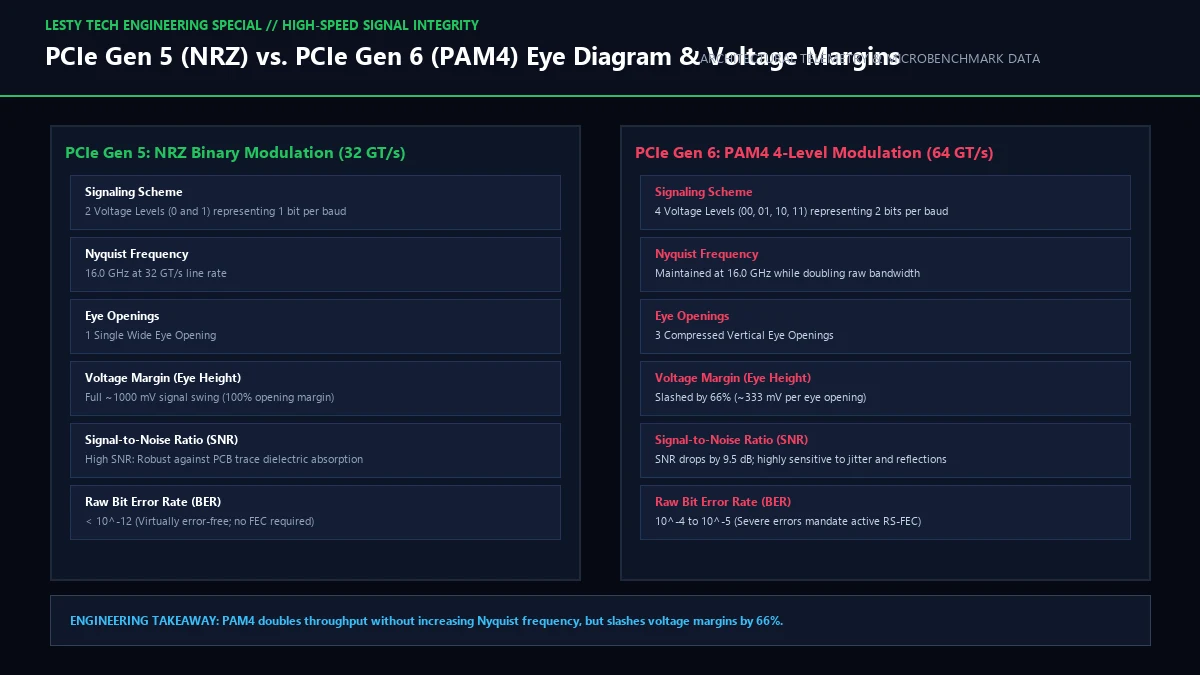
Because each symbol carries two full bits, the symbol transmission rate (the baud rate) for 64 GT/s is only 32 Gigabaud. Consequently, the fundamental Nyquist frequency remains locked at 16 GHzthe exact same frequency utilized by PCIe 5.0. Motherboards and connectors that successfully route PCIe 5.0 signals at 16 GHz can theoretically support PCIe 6.0 traces over similar physical distances without catastrophic dielectric absorption.
However, the physics of PAM4 introduces a devastating penalty: the SNR Collapse. In an oscilloscope eye diagram, an NRZ signal produces a single large vertical “eye” opening spanning the entire voltage differential (from -V to +V). In contrast, PAM4 must divide that exact same total voltage envelope into three stacked eye openings (between levels 0-1, 1-2, and 2-3).
Assuming an identical maximum transmitter output swing, the height of each PAM4 eye opening is mathematically exactly one-third (1/3) of the corresponding NRZ eye height. The loss in Signal-to-Noise Ratio is expressed logarithmically:
A 9.54 dB degradation in signal-to-noise ratio is monumental in high-speed hardware design. Small amounts of thermal jitter, power supply ripple, or crosstalk that were completely negligible in PCIe 5.0 NRZ can instantly corrupt a PAM4 symbol transition.
As a direct consequence, the Raw Bit Error Rate (BER) of the physical channel collapses. In PCIe 5.0, receivers were engineered to achieve a pristine raw BER of 10-12 (meaning no more than one corrupted bit in every one trillion bits transmitted). Under PCIe 6.0 PAM4, the raw channel BER degrades by seven to eight orders of magnitude down to 10-4 to 10-5meaning one corrupted bit every few tens of thousands of bits. At 64 Gbps, a raw BER of 10-4 produces millions of bit errors every single second.
3. The FLIT Revolution: Death of Variable-Length Packets
Because PCIe 6.0 physical channels produce millions of raw bit errors every second, the link would collapse immediately without an active mathematical error-correction system. However, classic Forward Error Correction (FEC) algorithms cannot operate on variable-length data streams with unpredictable boundaries.
In PCIe generations 1.0 through 5.0, data was packaged into variable-length Transaction Layer Packets (TLPs). A TLP could be anywhere from 20 bytes up to 4,096 bytes long, prepended with framing tokens (STP/END) and appended with a 32-bit Link CRC (LCRC). If an error occurred, the receiver detected it via CRC and issued a NAK, prompting the transmitter to replay the entire packet from its retry buffer.
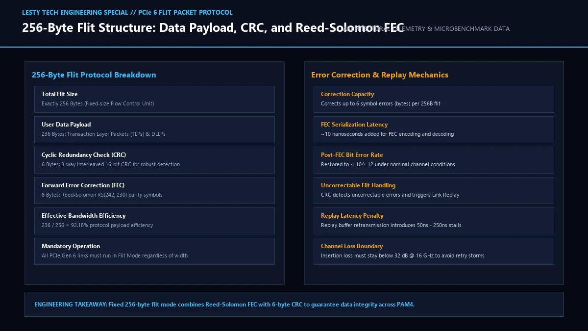
In PCIe 6.0, this entire 20-year-old framing architecture was scrapped. PCIe 6.0 completely eliminates framing tokens, start-of-packet markers, and variable packet boundaries at the physical layer. Instead, all data is strictly quantized into standardized, fixed-size Flow Control Units (FLITs). Every single FLIT is exactly 256 bytes (2,048 bits) in size:
[ 236 Bytes: Transaction Layer Payloads (TLPs) ]
[ 2 Bytes: Data Link Layer Payloads (DLP / Flow Control Credits) ]
[ 6 Bytes: Cyclic Redundancy Check (CRC-48) ]
[ 12 Bytes: Forward Error Correction Parity (FEC) ]
————————————————–
Total: 256 Bytes (2,048 bits)
By enforcing rigid 256-byte FLIT boundaries, the physical layer receiver knows the exact mathematical position of every data symbol and parity block in the incoming stream, enabling deterministic Forward Error Correction in hardware silicon.
4. The Lightweight FEC and the Sub-2-Nanosecond Latency Budget
In telecommunications and networking (such as 400G Ethernet), engineers solve PAM4 errors using heavy Reed-Solomon codessuch as RS(544, 514) KP4-FEC. While KP4-FEC provides massive error-correcting capability, it introduces a crushing decoding latency of 50 to 100 nanoseconds.
In networking, 100 nanoseconds of latency is completely imperceptible against wide-area internet delays. But in a computer architecture where a CPU is issuing loads across a PCIe/CXL bus to cache-coherent memory or GPU registers, 100 nanoseconds represents a catastrophic performance cliffdoubling or tripling the round-trip memory read latency.
To solve this, the PCI-SIG engineered a brilliant, highly specialized Lightweight Reed-Solomon FEC tailored specifically for PCIe 6.0. Rather than attempting to correct massive bursts of errors in a single code block, the PCIe 6.0 FEC operates on small 10-bit symbols with an ultra-short interleaving depth:
- 3-Way Interleaved RS Code: The 256-byte FLIT is partitioned into three independent, interleaved sub-blocks. Each sub-block can correct any single 10-bit symbol error within its domain.
- Low-Latency Hardware Decoding: Because the FEC code is mathematically lightweight, dedicated silicon decoders in modern PHYs (such as Synopsys or Cadence PCIe 6.0 controllers) can execute error correction in less than 1.5 to 2.0 nanoseconds.
- Fast-Path Latency Bypass: If a FLIT arrives at the receiver with zero bit errors detected (which occurs in over 99% of transmitted FLITs even with a 10-4 raw BER), the data payload can bypass the FEC decoding pipeline entirely, streaming directly into the host controller with sub-nanosecond processing delay.
However, if an electrical burst causes two or more symbol errors within a single interleaved sub-block, the lightweight FEC cannot correct them. This is where the 48-bit CRC (Cyclic Redundancy Check) and link-level replay engine intervene. When an uncorrectable multi-symbol error is flagged, the receiver immediately discards the damaged FLIT and transmits an ultra-low-latency replay request (NAK) back to the transmitter. The transmitter replays the missing 256-byte FLIT directly from its high-speed on-chip replay buffer.
This hybrid combination of a lightweight 2ns FEC and a fast hardware replay mechanism allows PCIe 6.0 to convert a raw channel BER of 10-4 into an effective post-FEC, post-replay Bit Error Rate of less than 10-27equivalent to less than one undetected data error every several hundred thousand years of continuous operation.
5. Complete Engineering Comparison: PCIe 4.0 vs 5.0 vs 6.0 vs 7.0
To visualize the massive technological leap represented by the transition to PAM4 and FLIT framing, review the detailed electrical and architectural specifications across generations:
| Architecture Metric | PCIe 4.0 (2017) | PCIe 5.0 (2019) | PCIe 6.0 (2022) | PCIe 7.0 (2025+) |
|---|---|---|---|---|
| Raw Transfer Rate | 16.0 GT/s | 32.0 GT/s | 64.0 GT/s | 128.0 GT/s |
| Signaling Modulation | NRZ (2-Level) | NRZ (2-Level) | PAM4 (4-Level) | PAM4 (4-Level) |
| Nyquist Frequency | 8.0 GHz | 16.0 GHz | 16.0 GHz (Unchanged) | 32.0 GHz |
| Bandwidth (x16 Slot) | 64 GB/s | 128 GB/s | 256 GB/s | 512 GB/s |
| Raw Channel BER Target | 10-12 | 10-12 | 10-4 to 10-5 | 10-4 to 10-5 |
| Packet Framing Mode | Variable TLP (128b/130b) | Variable TLP (128b/130b) | Fixed 256-Byte FLIT | Fixed 256-Byte FLIT |
| Forward Error Correction | None | None | Lightweight 3-Way RS FEC | Low-Latency RS FEC |
| Standard Board Material | Standard FR-4 / Mid-loss | Low-Loss (Megtron 4) | Ultra-Low-Loss (Megtron 6/8) | Next-Gen PTFE / Optical Hybrid |
6. Board Design Realities: Why Retimers Dominate the PCIe 6.0 Ecosystem
Although locking the Nyquist frequency at 16 GHz prevents a catastrophic jump in raw dielectric absorption, routing PCIe 6.0 signals on real-world printed circuit boards remains an extraordinarily challenging electrical feat.
Because the PAM4 eye height is only one-third that of NRZ, the maximum channel insertion loss budget allocated by the PCI-SIG remains fixed at -32 dB at 16 GHz across the entire channel (including the root complex package, motherboard trace, add-in card connector, and endpoint package). On a high-end enterprise motherboard built with premium ultra-low-loss dielectric substrates (such as Panasonic Megtron 6 or Nelco N4000-13), insertion loss averages approximately -1.2 dB to -1.5 dB per inch.
When you factor in connector losses (-2.5 dB) and package BGA pin transitions (-4 dB to -6 dB), the maximum reach of an unbuffered PCIe 6.0 trace is restricted to less than 10 to 14 inches. In massive multi-socket enterprise servers, GPU HGX chassis, and rack-scale CXL storage arrays, routing signals from a central CPU socket across baseboards and riser cards easily spans 20 to 30 inches.
To bridge this distance, PCIe 6.0 deployments rely extensively on active retimer chips (manufactured by companies like Astera Labs, Broadcom, and Marvell). A retimer is not a simple analog amplifier; it is a full physical-layer transceiver that deserializes the degraded PAM4 signal, reconstructs the digital bitstream through an internal CTLE (Continuous-Time Linear Equalizer) and DFE (Decision Feedback Equalizer), and re-transmits a pristine, jitter-free PAM4 signal down the next segment of the trace. In an 8-GPU AI server, up to sixteen PCIe 6.0 retimer chips are required, adding hundreds of dollars to the system bill of materials and dissipating an additional 100+ watts of localized power.
PCIe 6.0 PAM4 Signaling & Low-Latency FEC Whitepaper
Deep Engineering Analysis of 64 GT/s Modulation, 256-Byte FLITs, and Retimer Architectures (Complete architectural audit with telemetry tables and schematic breakdowns).
PCIe_Gen6_PAM4_Signaling_and_FEC_Overhead_Engineering_Dossier.pdfFormat: PDF / KaTeX Telemetry
Frequently Asked Questions (FAQ)
1. Is PCIe 6.0 backward compatible with older PCIe 4.0 and 5.0 graphics cards and SSDs?
Yes, 100%. Backward compatibility is a foundational tenet of the PCI-SIG specification. When a PCIe 5.0 or 4.0 device is plugged into a PCIe 6.0 slot, the physical layer executes a hardware link negotiation handshake during the initial training state (LTSSM). The PCIe 6.0 root complex detects that the endpoint does not support PAM4 or FLIT framing, automatically disables FEC, drops the modulation back to classic binary NRZ, and establishes the link at the highest common supported speed (e.g., 32 GT/s or 16 GT/s) with standard variable TLP framing.
2. Does the 256-byte FLIT structure waste bandwidth for small memory reads?
In traditional packet framing, sending a small 64-byte CPU cache line read required substantial relative header overhead (STP tokens, sequence numbers, 32-bit CRC). In PCIe 6.0 FLIT mode, small packets are aggregated and packed seamlessly across FLIT boundaries. Multiple TLPs can share a single 256-byte FLIT, or a large packet can span across multiple consecutive FLITs. While fixed framing introduces a theoretical 12-byte FEC parity overhead (roughly 4.7%), this is heavily offset by the complete elimination of legacy framing tokens and 128b/130b block headers, yielding a net protocol efficiency exceeding 95%.
3. Why didn’t PCIe 6.0 switch to optical interconnects instead of copper PAM4?
Cost, serviceability, and mechanical durability. While fiber optics have zero frequency attenuation over motherboard distances, optical transceivers (laser diodes, photodetectors, optical engines) are orders of magnitude more expensive than copper PCB traces. Furthermore, optical fiber connections in standard PC and server chassis are vulnerable to dust contamination, physical bending radius limits, and thermal degradation inside 80°C server chassis. Copper with PAM4 and active retimers remains significantly cheaper and robust enough to carry the industry through PCIe 6.0 and PCIe 7.0 before optical chiplets (CPO) become mandatory.