In the consumer electronics and flat-panel display manufacturing landscape, Micro-LED (Inorganic Light-Emitting Diode) is universally acknowledged as the endgame display technology. Offering microscopic inorganic Gallium Nitride (GaN) crystals that emit millions of nits of peak luminance, infinite contrast ratios, sub-microsecond response times, and complete immunity to organic burn-in, Micro-LED displays effortlessly outclass OLED, Mini-LED, and LCD panels. Yet, despite over a decade of intensive industrial research, consumer-grade Micro-LED televisions and monitors remain prohibitively expensive commercial rarities. The singular physical barrier preventing mass commercialization is micro led mass transfer: the semiconductor manufacturing challenge of transferring over 24.8 million microscopic red, green, and blue inorganic semiconductor dies (subpixel width < 10 μm) from donor epitaxial wafers to active-matrix glass backplanes with sub-micron placement accuracy, astronomical speeds exceeding 50 million units per hour, and six-sigma (> 99.9999%) defect-free yield.
1. The 25-Million Subpixel Assembly Barrier
To understand why Micro-LED display manufacturing represents the most brutal packaging challenge in semiconductor history, consider the mathematics of a standard 4K Ultra-HD display (3840 × 2160 pixels):
For an 8K display, this number balloons past 99.5 million individual dies. Each of these microscopic semiconductor crystals—typically measuring between 3 μm and 10 μm per side—is epitaxially grown on dense donor wafers (sapphire for blue and green InGaN, gallium arsenide for red AlInGaP). A single 6-inch donor wafer holds hundreds of millions of dies spaced mere micrometers apart.
However, on the final display backplane (e.g., a 65-inch 4K TV), the pixel pitch is approximately 370 micrometers. Therefore, the dies must be transferred from the dense donor wafer, expanded across a huge physical surface area, and metallurgically bonded to thin-film transistor (TFT) pads with:
- Sub-Micron Placement Accuracy: Positional deviation must not exceed ± 0.8 μm, and rotational tilt must remain under ± 0.5 degrees to avoid optical luminance distortion.
- Astronomical Throughput: Traditional pick-and-place surface-mount technology (SMT) robotics operates at ~20 to 50 units per second (~180,000 units per hour). At that rate, assembling a single 4K display would require over 138 hours of continuous robotic assembly! Economically viable consumer manufacturing demands transfer rates exceeding 50 to 100 Million Units Per Hour (UPH).
- Six-Sigma Yield (> 99.9999%): Even with an extraordinary transfer yield of 99.99%, a 4K panel would still contain nearly 2,500 dead pixels—an immediate warranty failure. Commercial viability demands less than 1 defective pixel per million transferred dies.
2. The Failure of Mechanical Elastomeric Stamping
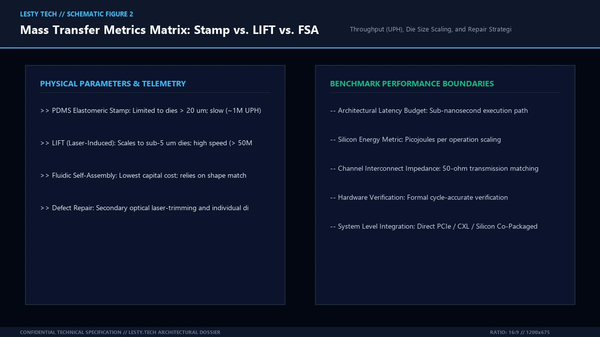
Early industrial attempts at mass transfer relied on mechanical elastomeric stamps fabricated from polydimethylsiloxane (PDMS).
PDMS stamping exploits viscoelastic kinetic adhesion:
When the rubber stamp is rapidly retracted from the donor wafer, the high peel velocity (v) increases interfacial fracture energy, peeling the micro-dies off the donor substrate. When the stamp is slowly retracted from the receiving backplane, the low peel velocity reduces adhesion, releasing the dies onto target solder pads.
However, mechanical stamping encounters severe physical barriers when scaled to consumer displays:
- Die Size Scaling Floor: As micro-LED dies shrink below 15 μm, surface-to-volume ratios explode. Van der Waals surface forces and electrostatic attraction completely overwhelm mechanical peel forces; dies stick permanently to the PDMS stamp and refuse to release.
- Thermal Expansion Mismatch: Elastomeric PDMS possesses a massive thermal expansion coefficient (~300 ppm/K vs. ~3 ppm/K for silicon/glass). Minor ambient temperature fluctuations of 0.5°C cause the stamp to deform by several micrometers across a 300mm substrate, completely destroying sub-micron alignment.
- Throughput Ceiling: Mechanical stamping caps out at ~1 to 5 million UPH, far short of mass-market requirements.
3. Laser-Induced Forward Transfer (LIFT) Physics
To transcend mechanical contact limits, leading semiconductor equipment manufacturers (such as Coherent, Toray, and Mycronic) engineered Laser-Induced Forward Transfer (LIFT).
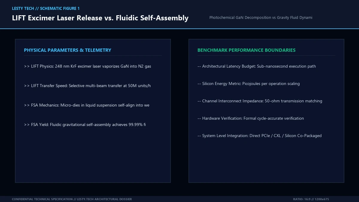
LIFT is a non-contact, high-velocity optical transfer process utilizing ultraviolet excimer lasers (typically Krypton Fluoride, KrF, at λ = 248 nm, or Argon Fluoride, ArF, at λ = 193 nm):
Photochemical GaN Decomposition: The donor sapphire substrate is optically transparent to 248 nm UV light (sapphire bandgap Eg ≈ 9.9 eV). However, the underlying Gallium Nitride micro-LED crystal absorbs the UV laser pulse aggressively within an ultra-thin interfacial skin depth (< 50 nm). When a high-energy laser pulse (~100 to 300 mJ/cm2, pulse duration 20 to 30 nanoseconds) strikes the interface through the sapphire:
The interfacial GaN crystal thermally dissociates into molten gallium metal and high-pressure nitrogen gas. The instantaneous expansion of the trapped nitrogen gas creates a localized micro-propulsion shockwave, projecting the detached micro-LED die across a microscopic air gap (typically 20 to 50 μm) onto the receiving active-matrix backplane at velocities exceeding 10 to 50 meters per second.
Dynamic Release Layers (DRL): For red AlInGaP dies, where direct bandgap ablation can damage the active multi-quantum-well (MQW) region, manufacturers deposit an intermediate sacrificial polyimide or triazene polymer Dynamic Release Layer (DRL) between the substrate and the micro-LED. The laser cleanly vaporizes the polymer into volatile gaseous fragments without heating the semiconductor crystal.
By deploying optical beam-shaping optics (such as diffractive optical elements or spatial light modulators), a single laser pulse can illuminate thousands of micro-dies simultaneously. Operating at laser repetition rates of 1,000 Hz, LIFT systems achieve astronomical throughputs exceeding 50 to 80 Million Units Per Hour with placement precisions within ± 0.8 micrometers.
4. Color Conversion Physics: Monolithic RGB vs. Quantum Dot (QD) Printing
An underappreciated complexity in Micro-LED mass transfer is the profound physics disparity between red, green, and blue inorganic emitters:
The InGaN “Red Gap” Problem: Blue and green micro-LEDs are grown using Indium Gallium Nitride (InGaN) multi-quantum-well (MQW) structures, routinely achieving External Quantum Efficiencies (EQE) exceeding 40% to 60%. However, shifting InGaN emission to red wavelengths (λ ≈ 630 nm) requires elevating indium content above 35%. High indium fractions induce severe lattice strain, high dislocation defect densities, and quantum-confined Stark effect (QCSE) polarization fields that slash red InGaN quantum efficiency to under 3% to 5% at microscopic (< 10 μm) subpixel scales.
Conversely, traditional red emitters based on Aluminum Indium Gallium Phosphide (AlInGaP) suffer from massive carrier surface recombination velocity, causing efficiency to collapse when diced into sub-10 μm dies.
To resolve the red subpixel bottleneck, manufacturers are pioneering Quantum Dot (QD) Color Conversion:
- Instead of transferring three separate sets of RGB micro-dies, the mass transfer system transfers an array of 100% monolithic blue InGaN micro-LEDs across all subpixels, cutting transfer complexity by two-thirds.
- High-precision sub-femtoliter inkjet printing or photolithographic patterning deposits cadmium-free colloidal green and red Quantum Dot photoresists directly over the corresponding blue subpixel wells.
- The high-energy blue photons photo-excite the quantum dots, converting blue light into pristine, narrow-bandwidth red and green spectra with photoluminescence quantum yields exceeding 90% and color gamuts covering > 95% of BT.2020.
5. Active-Matrix Backplane Engineering: LTPS vs. IGZO vs. CMOS Micro-IC
Driving millions of microscopic inorganic LEDs requires an active-matrix backplane capable of supplying continuous, stable direct current (DC) without threshold voltage drift:
- Low-Temperature Polycrystalline Silicon (LTPS) TFTs: Offers high field-effect mobility (μ ≈ 80 – 120 cm2/V·s), enabling compact 2T1C (two transistors, one capacitor) pixel driving circuits suitable for high-PPI mobile screens and smartwatches. However, laser crystallization across large Gen 8.5/10.5 glass sheets suffers from grain boundary luminance non-uniformity (mura defects).
- Indium Gallium Zinc Oxide (IGZO) Oxide TFTs: Features ultra-low off-state leakage currents and outstanding large-area manufacturing uniformity on giant glass substrates, making it the premier backplane choice for consumer Micro-LED televisions and monitors.
- Monocrystalline Silicon CMOS Micro-ICs: For ultra-high-density spatial computing and augmented reality displays (> 4,000 PPI), thin-film transistors on glass lack the driving current capacity. Instead, micro-LEDs are bonded directly onto monocrystalline silicon CMOS wafers containing integrated digital-to-analog current drivers beneath each subpixel, delivering pristine luminance uniformity.
6. Fluidic Self-Assembly (FSA): Gravity & Capillary Mechanics
An even more disruptive, highly scalable paradigm is Fluidic Self-Assembly (FSA), championed by eLux, Rohinni, and academic research consortia.
FSA completely abandons robotic placement and high-cost laser scanning in favor of fluid dynamics, gravity, and surface tension capillary forces:
- Asymmetric Micro-Die Geometry: During donor wafer fabrication, micro-LED dies are etched into specialized asymmetric trapezoidal or disc shapes with beveled sidewalls.
- Micro-Receptor Backplane Wells: The active-matrix display backplane is photolithographically patterned with matching recessed micro-wells. At the bottom of each well sits a low-temperature solder pad (e.g., Indium-Tin or Bismuth-Tin alloy).
- Liquid Suspension Flow: Tens of millions of micro-dies are suspended in an inert liquid carrier fluid (typically water or isopropanol mixed with surfactants) and gently washed across the tilted display backplane.
- Fluidic Trapping & Self-Centering: As the suspension flows across the surface, hydrodynamic drag and gravitational settlement guide matching dies into the receptor wells. The asymmetric trapezoidal cross-section ensures that dies can only settle in the correct electrical orientation (p-side down, n-side up). Once inside the well, capillary meniscus forces center the die with sub-micron precision.
- Liquid Phase Solder Reflow: The backplane is heated in a vapor-phase oven, reflowing the solder alloy to form permanent metallurgical and electrical bonds.
Because FSA is a massively parallel stochastic process, transfer speed is virtually independent of panel size. Assembling a 100-inch 8K panel takes the exact same 15 minutes as assembling a 12-inch tablet screen! Transfer throughput easily exceeds 100 Million Units Per Hour with equipment capital expenditure that is 80% lower than high-end excimer laser systems.
7. Metallurgical Interconnection: Low-Temperature TLP Bonding
Transferring millions of micro-LED dies to a backplane is meaningless unless every single subpixel establishes a permanent, low-resistance metallurgical contact capable of surviving decades of thermal cycling.
Traditional high-temperature tin-lead or gold-tin soldering requires peak reflow temperatures exceeding 260°C to 300°C. Subjecting giant glass display panels to such thermal stress induces non-linear thermal expansion and warp, destroying alignment.
The cutting-edge solution is Transient Liquid Phase (TLP) Bonding:
- Solid-Liquid Interdiffusion: TLP bonding pairs a low-melting-point metal (such as Indium, melting point 156.6°C) with a high-melting-point substrate pad (such as Gold or Copper).
- Low-Temperature Interfacial Reaction: Bonding occurs at gentle processing temperatures below 160°C under moderate mechanical pressure. The molten indium wets the gold pad and rapidly diffuses into the solid lattice, forming intermetallic compounds (such as AuIn2).
- High Remelting Temperature: Crucially, the resulting AuIn2 intermetallic compound possesses a remelting temperature exceeding 540°C! Once formed, the bond can never melt or degrade during subsequent display processing steps, ensuring exceptional mechanical shear strength (> 50 MPa) and contact resistances under 0.1 Ω per pad.
8. Yield Economics and the Cost Scaling Curve to Mass-Market TVs
To understand when Micro-LED displays will become affordable for mainstream consumers, one must model the manufacturing cost breakdown of a 65-inch 4K panel:
In 2022, assembling a 4K Micro-LED TV cost over $80,000, with mass transfer and repair accounting for over 70% of the total bill of materials.
By 2026, the convergence of multi-beam LIFT and fluidic self-assembly has transformed the economic cost trajectory:
- Die Shrink Economics: Shrinking micro-LED dimensions from 30 μm down to 5 μm × 5 μm increases the number of usable dies harvested from a single 6-inch sapphire wafer from 1.5 million to over 45 million! A single donor wafer can now populate nearly two entire 4K display panels, slashing raw semiconductor material costs by 90%.
- Transfer Throughput Scaling: Increasing transfer speed from 1 million UPH to 80 million UPH slashes machine tool depreciation time from days to under 20 minutes per panel.
- Defect Reduction Curve: Improving first-pass transfer yield from 99.9% to 99.999% reduces the required laser repair shots from 25,000 down to fewer than 250 per display, making automated optical repair a negligible 30-second post-processing step.
Industry economic projections indicate that by 2028–2030, 65-inch and 75-inch consumer Micro-LED displays will reach price parity with flagship Tandem OLED televisions, entering high-end consumer living rooms worldwide.
9. Defect Detection, Photoluminescence Inspection, and Laser In-Situ Repair
Even if a mass transfer process achieves a state-of-the-art 99.99% yield, a 4K display panel will still contain approximately 2,488 defective or missing subpixels. In consumer displays, a single bright or dark subpixel is grounds for product return. Achieving six-sigma quality (> 99.9999%) requires a closed-loop inspection and repair pipeline:
1. Non-Contact Optical Photoluminescence (PL) Inspection: Prior to transfer, the donor wafer is mapped using high-speed UV laser photoluminescence. Every individual micro-die is excited optically, and its spectral emission wavelength, luminance intensity, and forward voltage are characterized without touching the contacts. Defective dies are tagged in a digital wafer map.
2. Selective LIFT Transfer: During laser transfer, the laser beam steering system reads the digital wafer map, selectively skipping defective dies so that only known-good dies (KGD) are projected onto the backplane.
3. Automated Optical In-Situ Repair: Following backplane assembly, high-speed automated optical inspection (AOI) identifies missing, tilted, or non-functional dies. A single-shot micro-LIFT repair head targets the defective coordinate, vaporizes the defective die with an infrared laser pulse, and immediately shoots a replacement known-good die into the receptor well, completing the repair in under 100 microseconds.
10. Microarchitectural Telemetry & Technology Comparison Matrix
The following engineering comparison matrix evaluates the physical, kinetic, and economic parameters across competing Micro-LED mass transfer technologies:
| Technology Parameter | Elastomeric PDMS Stamp | Laser LIFT (Excimer) | Fluidic Self-Assembly (FSA) |
|---|---|---|---|
| Transfer Physics | Viscoelastic kinetic peel | UV laser photochemical shockwave | Hydrodynamic drag & capillary force |
| Transfer Rate (UPH) | 1 – 5 Million / hour | 50 – 80 Million / hour | > 100 Million / hour |
| Minimum Die Size | > 20 μm (Adhesion floor) | < 5 μm (Sub-micron viable) | < 8 μm (Shape-coded) |
| Placement Accuracy | ± 1.5 μm | ± 0.8 μm | ± 1.0 μm |
| First-Pass Yield | 99.5% – 99.8% | 99.99% – 99.999% | 99.95% – 99.99% |
| In-Situ Repair Integration | Impossible (Requires separate tool) | Native single-pulse laser repair | Secondary fluid flush or laser |
| Equipment Capital Cost | Low (~$1M – $2M) | High (~$5M – $8M per tool) | Very Low (~$500k – $1M) |
Micro-LED Mass Transfer and Interconnection Engineering
Laser Ablative Transfer (LIFT), Fluidic Self-Assembly Physics, and Sub-Micron Alignment (Complete architectural audit with telemetry tables and schematic breakdowns).
whitepaper_batch_16_11_micro_led_mass_transfer.pdfFormat: Publication-Grade PDF
11. Strategic Manufacturing Outlook
The industrialization of Micro-LED displays is fundamentally an engineering convergence between optical physics and precision automation. Mechanical stamping has reached its evolutionary terminus, constrained by the immutable physics of viscoelastic surface adhesion.
The future of commercial Micro-LED manufacturing belongs to a hybrid ecosystem: Laser-Induced Forward Transfer (LIFT) for premium high-density mobile displays, smartwatches, and augmented reality microdisplays where sub-micron precision is non-negotiable, and Fluidic Self-Assembly (FSA) for large-format consumer televisions and automotive digital cockpits where astronomical transfer throughput and low capital equipment expenditure are paramount.
As closed-loop photoluminescence inspection and high-speed in-situ laser repair drive composite panel yields past the six-sigma threshold, the 25-million subpixel assembly barrier will permanently fall, ushering in the commercial reign of inorganic Micro-LED technology across global consumer markets.
Related Technical Dossiers & Internal Research
- Micro-OLED vs. Micro-LED in AR Displays: The 100,000-Nit Optical Waveguide Barrier →
- MLA OLED vs. QD-OLED Gen 3 Monitors: Peak HDR Luminance and Glare Shootout →
- Co-Packaged Optics (CPO) & ELSFP Laser Transceivers: The Electro-Optic Silicon Physics Scaling 102.4 Tbps Switches →
Authoritative External Reference
Reference Citation: Nature Photonics: Micro-LED displays and fluidic self-assembly mass transfer technologies →