In the consumer electronics landscape, the race to build the successor to the smartphone has converged on a single physical form factor: lightweight, all-day augmented reality (AR) smart glasses. Unlike bulky virtual reality (VR) and mixed-reality (MR) visors like the Apple Vision Pro or Meta Quest 3—which isolate the user behind opaque enclosures and display digitized camera pass-through video—true optical AR glasses must project full-color digital typography, navigational overlays, and spatial computing interfaces directly onto transparent glass through which the physical world remains naturally visible. But delivering this visual experience encounters the most brutal photonics bottleneck in optical physics: the Optical Waveguide Attenuation Wall. Planar diffractive surface-relief waveguides lose more than 98% to 99% of all injected light before photons ever reach the human retina. Evaluating micro oled vs micro led microdisplays exposes a stark technological schism. While silicon-backplane Micro-OLED delivers flawless contrast and 4K subpixel density in dark VR headsets, its organic emitters cap out at 5,000 nits, turning into an invisible, washed-out ghost under sunlight. Conversely, inorganic Gallium Nitride (GaN) Micro-LED delivers over 1,000,000 nits of raw optical power to conquer outdoor glare, but battles microscopic subpixel quantum efficiency dropoffs, the infamous “Red Gap,” and severe color conversion hurdles.
1. The Optical Waveguide Efficiency Bottleneck
To understand why augmented reality demands display luminance levels orders of magnitude beyond televisions or smartphones, one must analyze the optical physics of planar diffractive waveguides.
In a transparent AR display, the image generator (light engine) cannot sit directly in front of the human eye without blocking external vision. Instead, the microdisplay engine is mounted discreetly inside the temple frame of the glasses. To transfer light from the side of the glasses into the user’s line of sight, the system utilizes a flat optical plate made of high-refractive-index glass (n ≈ 1.9 to 2.1) or optical-grade silicon carbide.
The propagation of light through a surface-relief diffractive waveguide follows a multi-stage optical path governed by the grating equation:
Where θm is the diffracted angle, θin is the incident angle, m is the diffraction order (m = ±1), λ is the wavelength of light, and Λ is the nanoscale grating pitch etched into the surface.
The optical journey through the waveguide incurs staggering photon loss at every transition:
- Input Coupling Grating (ICG): Microdisplay photons strike the input grating to be diffracted at an angle exceeding the critical angle (θc = arcsin(1/n)), trapping the light within the glass via Total Internal Reflection (TIR). Input coupling efficiency is typically only 15% to 25%; the remaining light reflects into space or scatters.
- Fold Grating (Pupil Expansion): To provide a comfortable viewing area (eyebox) so the image doesn’t vanish when the glasses shift on the user’s face, light bounces through a fold grating that expands the beam along the horizontal and vertical axes. Multiple internal reflections incur Fresnel scattering and polarization-dependent transmission losses, stripping another 50% to 70% of optical power.
- Output Coupling Grating (OCG): The expanded beam strikes the output grating, diffracting light out of Total Internal Reflection and directing it into the user’s pupil. Output grating extraction efficiency is intentionally low (1% to 3%) across the eyebox surface to maintain uniform illumination.
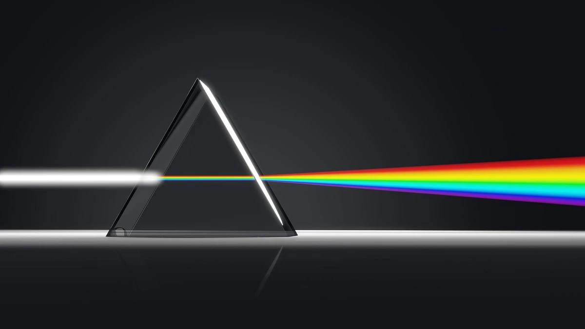
When all optical transmission coefficients are multiplied across the full red, green, and blue optical spectrum, the total end-to-end optical efficiency (ηwaveguide) of commercial diffractive waveguides is shockingly poor:
Now, consider the ambient illumination of the physical world. On a bright, sunny afternoon in direct sunlight, ambient horizontal illuminance reaches 10,000 to 100,000 lux. For digital text and spatial UI overlays to remain legible against bright concrete or sky, the display must achieve a contrast ratio of at least 5:1, requiring a minimum eye-level luminance of 1,000 to 2,000 nits delivered into the pupil.
Calculating the required microdisplay engine surface luminance (\(L_{\text{engine}}\)):
An augmented reality smart glasses display engine must emit an astonishing 100,000 to 200,000 nits of raw optical luminance at the silicon surface just to deliver a crisp, readable 1,500 nits through a diffractive waveguide outdoors!
2. Micro-OLED (OLEDoS): The VR Champion Trapped by Organic Physics
Micro-OLED (often referred to as OLED-on-Silicon or OLEDoS) represents the pinnacle of virtual reality and pass-through mixed-reality display engineering. Pioneered by Sony and prominently showcased in the Apple Vision Pro (featuring twin 1.42-inch 4K panels with 23 million pixels), Micro-OLED differs fundamentally from consumer smartphone OLED displays.
Instead of depositing organic thin-film transistors onto flexible polyimide or glass substrates, Micro-OLED evaporates organic emissive materials directly onto a monocrystalline silicon wafer CMOS backplane. Monocrystalline silicon provides sub-micron transistor channel lengths, allowing foundries to pack subpixels at pitches below 3.5 micrometers, yielding extreme pixel densities exceeding 3,500 to 4,000 Pixels Per Inch (PPI).
Because every subpixel is an independent organic light-emitting diode, Micro-OLED provides:
- True inky blacks (luminance < 0.0001 nits) with infinite contrast ratios (> 1,000,000:1).
- Zero blooming, haloing, or localized backlight bleed.
- Sub-millisecond pixel response times (under 50 microseconds), eliminating motion blur and VR motion sickness.
However, when applied to transparent diffractive AR waveguides, Micro-OLED encounters a catastrophic physical barrier: organic material thermal degradation.
In a Micro-OLED stack, light is generated by the radiative recombination of excitons (bound electron-hole pairs) within organic molecular emitter layers. As electrical current density (J) is scaled up to boost brightness, exciton density spikes. Above critical thresholds, excitons undergo non-radiative quenching processes—specifically triplet-triplet annihilation (TTA) and singlet-polaron quenching (SPQ):
This exciton annihilation transforms electrical energy into localized Joule heat rather than photons, accelerating the chemical dissociation of organic carbon-nitrogen covalent bonds. Driving a single-stack Micro-OLED panel past 5,000 nits causes instantaneous efficiency collapse and permanent pixel burn-in within hundreds of operating hours.
Advanced tandem architectures (stacking two or three organic PIN junctions in series connected by intermediate charge generation layers) improve efficiency, pushing peak luminance to approximately 10,000 to 12,000 nits. However, when paired with a diffractive waveguide exhibiting 1% optical efficiency:
An eye-level brightness of 120 nits is washed out and completely invisible against outdoor ambient lighting (5,000 to 50,000 lux). Micro-OLED is physically confined to dark VR headsets and indoor MR visors; it cannot power all-day transparent outdoor AR smart glasses.
3. Micro-LED (LEDoS): Inorganic Semiconductor Optical Supremacy
To overcome the organic thermal limits of Micro-OLED, display engineers developed Micro-LED (LEDoS, or LED-on-Silicon). Unlike organic materials, Micro-LED relies on robust inorganic semiconductor crystals—predominantly Indium Gallium Nitride (InGaN) and Aluminum Indium Gallium Phosphide (AlInGaP)—grown epitaxially on sapphire or silicon substrates.
Inorganic semiconductor crystals possess immense bond energies and thermal conductivity orders of magnitude higher than organic plastics. Micro-LEDs can withstand electrical current densities exceeding 1,000 A/cm2 without chemical degradation.
The result is an extraordinary leap in optical luminance:
- Green InGaN Micro-LED microdisplays routinely generate over 2,000,000 to 5,000,000 nits of raw surface brightness.
- Blue InGaN Micro-LED engines produce over 1,000,000 nits.
- Full-color monolithic RGB Micro-LED arrays deliver sustained outputs between 100,000 and 1,000,000 nits.
When paired with an optical waveguide experiencing 99% photon loss, a 1,000,000-nit Micro-LED engine delivers 10,000 nits directly to the eye—more than enough to display razor-sharp, high-contrast navigation graphics against midday summer skies or sunlit snow. Furthermore, because inorganic GaN is completely immune to organic photo-oxidation, operational lifespan exceeds 50,000 to 100,000 hours without pixel degradation.
This was the decisive architectural factor that led Meta to choose custom Silicon-Carbide waveguides paired with Micro-LED projectors for its groundbreaking Orion AR smart glasses prototype in 2024.
Beyond raw luminance, inorganic Micro-LED offers an astonishing switching response time of less than 1 nanosecond (compared to 10 to 50 microseconds for Micro-OLED). This extreme response speed enables ultra-high frame rate pulse-width modulation (PWM) driving schemes (exceeding 10,000 Hz) and allows advanced pupil-tracking foveated rendering engines to eliminate stroboscopic artifacts, temporal tearing, and retinal ghosting during rapid ocular saccades.
4. The Manufacturing Nightmares: The “Red Gap” & Sidewall Defects
If Micro-LED possesses such decisive optical superiority, why hasn’t it completely replaced Micro-OLED across every display on earth? The answer lies in two catastrophic physical manufacturing bottlenecks: The Red Gap and Sidewall Non-Radiative Recombination.
The Red Gap: InGaN semiconductors excel at emitting high-energy blue (450 nm) and green (525 nm) photons, achieving Internal Quantum Efficiencies (IQE) exceeding 60% to 80%. However, producing red light (630 nm) requires increasing the Indium fraction in the InGaN quantum wells to over 35%. Because Indium atoms have a much larger atomic radius than Gallium, this high concentration induces extreme lattice strain and piezoelectric polarization fields (the Quantum-Confined Stark Effect, QCSE). As a result, red InGaN quantum efficiency collapses to less than 5% to 8%! Traditional red emitters use AlInGaP materials, but AlInGaP possesses a long carrier diffusion length, causing efficiency to collapse to near-zero when dies are shrunk below 5 microns.
Sidewall Non-Radiative Recombination: To achieve 4K resolution on a 0.2-inch microdisplay, each individual Micro-LED die must be shrunk down to a subpixel pitch of sub-2.0 micrometers. Etching millions of microscopic LED mesas using Reactive Ion Etching (ICP-RIE) inflicts severe atomic damage along the vertical sidewalls of the semiconductor crystal. Dangling bonds and crystal lattice vacancies act as electron-hole recombination traps:
As die width wdie shrinks below 3 microns, the surface-to-volume ratio explodes. Injected electrons and holes migrate to the damaged sidewalls and recombine without emitting light, draining up to 70% of injected electrical power into heat. Overcoming sidewall defects requires atomic layer deposition (ALD) dielectric passivation and chemical wet-etch healing, demanding unprecedented semiconductor lithographic precision.
The Color Conversion Dilemma: QDCC vs. Monolithic 3D Stacking: To circumvent the Red Gap, display foundries are pursuing two radical fabrication architectures:
- Quantum Dot Color Conversion (QDCC): Instead of fabricating native red and green micro-LEDs, foundries fabricate a monolithic array of uniform, high-efficiency blue InGaN micro-LEDs. Sub-micron inkjet printing or photolithographic patterning then deposits red and green colloidal Cadmium-free quantum dots onto adjacent subpixels. The blue pump photons excite the quantum dots, converting blue light into vibrant red (630 nm) and green (530 nm) with narrow Full-Width at Half-Maximum (FWHM < 30 nm). However, quantum dots degrade under high heat and intense photon flux, limiting sustained engine luminance to approximately 250,000 nits.
- Wafer-to-Wafer Direct Cu-Cu Hybrid Bonding: The ultimate optical solution involves vertically stacking three distinct InGaN/AlInGaP epitaxial layers (Red, Green, and Blue) grown on individual wafers and bonding them directly to a CMOS silicon driver wafer using ultra-high-precision Copper-Copper (Cu-Cu) dielectric hybrid bonding. With bonding pad pitches scaled down to sub-1.5 micrometers, alignment tolerance must stay within ±0.2 micrometers across the entire 300 mm wafer. While this delivers full-color output exceeding 1,000,000 nits without color filters or quantum dots, current cleanroom yields remain below 30%, making production costs astronomical.
| Display Technology | Peak Surface Luminance | Optical Eye Luminance (1% Waveguide) | Outdoor Sunlight Legibility | Manufacturing Maturity & Yield |
|---|---|---|---|---|
| Standard Silicon Micro-OLED | 3,000 – 5,000 nits | 30 – 50 nits | Invisible (Unusable Outdoors) | High (Commercial Production) |
| Tandem Dual-Stack Micro-OLED | 10,000 – 12,000 nits | 100 – 120 nits | Marginal (Indoor / Shaded Only) | Medium (Pilot Commercial) |
| Monochrome Green Micro-LED | 2,000,000 – 5,000,000 nits | 20,000 – 50,000 nits | Flawless Sunlight Visibility | Commercial (HUD / Smart Glasses) |
| Full-Color Monolithic Micro-LED | 150,000 – 1,000,000 nits | 1,500 – 10,000 nits | Perfect Outdoor Readability | Low (Pilot Wafers / Active R&D) |
5. The Architectural Divergence: VR vs. True Optical AR
This physical comparison establishes a permanent, immutable bifurcation in spatial computing hardware architecture:
Virtual Reality & Pass-Through Mixed Reality: Micro-OLED Is King. For headsets like the Apple Vision Pro, Meta Quest Pro 2, and high-end flight simulators, the display operates inside a closed, dark cavity. Optical lenses (such as folded polarization pancake optics) transmit 15% to 25% of light—twenty times more efficient than diffractive waveguides. Under these conditions, a 3,000-nit Micro-OLED panel delivers a stunning 500 nits to the user’s eye. Micro-OLED provides true zero-luminance blacks for movie watching, flawless color grading, zero haloing, and cost-effective 4K CMOS scaling. Micro-LED has virtually zero advantage in VR headsets and cannot compete on subpixel cost.
Transparent Optical Augmented Reality Glasses: Micro-LED Is Non-Negotiable. For all-day smart glasses resembling standard Ray-Ban frames with transparent lenses, Micro-OLED is a non-starter. No amount of software optimization can overcome the fundamental laws of waveguide diffraction. Micro-LED is the only display technology capable of delivering 1,000,000 nits of surface luminance, ensuring that turn-by-turn navigation arrows, incoming messages, and contextual AI annotations remain vivid under intense summer sunlight.
Micro-OLED vs. Micro-LED in Augmented Reality: Optical Waveguide Attenuation and Microdisplay Physics
Display Engineering Analysis of Waveguide Diffraction Losses, 100,000-Nit Luminance, and Subpixel Pitch (Complete architectural audit with telemetry tables and schematic breakdowns).
Micro_OLED_vs_Micro_LED_in_Next_Gen_AR_Waveguide_Displays_Dossier.pdfFormat: Publication-Grade PDF
6. Consumer Buying Advice & Industry Horizon (2026–2028)
For consumers, developers, and enterprise hardware buyers evaluating spatial computing investments across 2026 and 2027:
1. Beware Marketing Claims of “Micro-LED” on Consumer Glasses: Many affordable smart glasses advertised online as “Micro-LED” are in reality utilizing single-color green projectors (useful only for green text notification tickers) or are mislabeling standard Micro-OLED panels. A true, full-color monolithic RGB Micro-LED smart glasses product remains in prototype and restricted enterprise developer kit stages.
2. Expect Two Distinct Hardware Generations: In the interim, expect smart glasses manufacturers to deploy two complementary tiers:
- Tier 1: Monochrome Green Micro-LED (Current 2026 Reality): Ultra-lightweight 50-gram glasses with 20,000-nit eye brightness, delivering 18-hour battery life for AI voice assistant prompts, translation, and teleprompter cues.
- Tier 2: Full-Color Quantum Dot Micro-LED (2027–2028 Horizon): Utilizing native blue InGaN arrays covered with printed sub-micron red and green colloidal quantum dots, bypassing the Red Gap to deliver full-color augmented reality at consumer scale.
7. Frequently Asked Questions (FAQ)
Why do augmented reality waveguides lose so much light?
Diffractive surface-relief waveguides rely on nanoscale gratings to inject, expand, and extract light via Total Internal Reflection (TIR). Due to polarization scatter, high-angle diffraction limits, and intentional low extraction efficiency to maintain a uniform eyebox across the user’s vision, more than 98% of light is scattered or lost, delivering only 1% to 2% of emitted photons to the eye.
Why can’t manufacturers just drive Micro-OLED panels at 100,000 nits?
Micro-OLED utilizes organic electroluminescent molecules. When driven with high current densities, exciton quenching (triplet-triplet annihilation and singlet-polaron quenching) converts electrical energy into localized heat, destroying the organic chemical bonds and causing catastrophic pixel burn-in within hours. Even tandem dual-stack Micro-OLED caps out at roughly 12,000 nits.
What is the “Red Gap” in Micro-LED manufacturing?
Indium Gallium Nitride (InGaN) crystals emit blue and green light with high efficiency (>60%), but producing red light requires high Indium concentrations that warp the crystal lattice, causing quantum efficiency to collapse to less than 8%. While AlInGaP materials produce red light efficiently in large sizes, their efficiency crashes when dies are shrunk below 5 microns due to long carrier diffusion lengths.
Why does the Apple Vision Pro use Micro-OLED instead of Micro-LED?
The Apple Vision Pro is an enclosed VR/MR headset that uses pancake optics rather than transparent diffractive waveguides. Pancake lenses transmit 20x more light than waveguides, requiring only 5,000 nits from the display. Micro-OLED provides true blacks, sub-3.5um pixel pitches for 4K per eye, and mature wafer-scale manufacturing that Micro-LED cannot match today.
When will full-color Micro-LED AR glasses become widely available to consumers?
Monochrome green Micro-LED smart glasses are already in limited commercial production. Full-color monolithic RGB Micro-LED glasses (like the consumer descendants of Meta’s Orion prototype) are expected to reach commercial consumer retail between 2027 and 2028 as quantum dot color conversion (QDCC) and wafer-scale bonding yields mature.
Related Technical Dossiers & Internal Research
- QD-OLED vs. WOLED in 2026 Monitors: The Subpixel Fringing Physics, Glare Coatings, and Text Clarity Shootout
- DisplayPort 2.1 UHBR Speed Ratings: The Bandwidth Physics Powering 8K 240Hz
- Diamond Heat Spreaders & Heterogeneous GaN Integration: The Phonon Transport Physics Dissipating 2,000 W/cm² in AI Power Dies
Authoritative External Reference
Reference Citation: Society for Information Display (SID) Display Week: Advances in Micro-LED and Diffractive Waveguides →





No Responses