
In hyperscale AI datacenter clusters scaling to tens of thousands of interconnected GPUs, network switching infrastructure has collided with a catastrophic electro-optic physics bottleneck: the Copper SerDes Attenuation Wall. As aggregate network switch bandwidth escalates from 51.2 Tbps to 102.4 Tbps, driving 224 Gbps-per-lane electrical signals across standard printed circuit board (PCB) traces incurs over 30 dB of high-frequency insertion loss, devouring more than 40% of the entire switch chassis power budget just to equalize electrical channels. Co-Packaged Optics (CPO) resolves this by mounting silicon photonic optical engines directly onto the switch substrate beside the compute ASIC. Yet, integrating fragile semiconductor laser diodes directly onto a 1,000-watt silicon substrate creates severe thermal runaway and Mean Time Between Failures (MTTF) collapse. To solve this, industry standards have converged on the copackaged optics elsfp laser architecture. By isolating high-power continuous-wave (CW) Distributed Feedback (DFB) laser arrays inside front-panel hot-pluggable modules, ELSFP enables sub-5.5 pJ/bit optical transmission while ensuring multi-million-hour laser reliability.
1. The 102.4T Interconnect Bottleneck: Copper Attenuation vs. Power Density
Modern cloud AI clusters training trillion-parameter foundation models depend on ultra-low latency, non-blocking network fabrics. In traditional switch designs, a monolithic switch ASIC sits at the center of a massive multi-layer PCB, routing hundreds of high-speed differential pairs across 10 to 18 inches of board laminate to front-panel pluggable optical transceivers (such as OSFP or QSFP-DD modules).
At PAM4 signaling rates of 112 Gbps per lane (56 GBaud Nyquist frequency at 28 GHz), high-frequency dielectric losses in advanced Megtron-7 or Tachyon PCB materials are already severe (~18 to 22 dB insertion loss). When scaling to next-generation 224 Gbps per lane (112 GBaud Nyquist frequency at 56 GHz), dielectric skin effect and material dissipation factors skyrocket:
Where f is the signaling frequency (56 GHz), \(\varepsilon_r\) is relative dielectric permittivity, \(\tan \delta\) is the loss tangent, w is trace width, and \(\sigma\) is copper conductivity. Over an 18-inch reach, total insertion loss exceeds 32 to 38 dB.
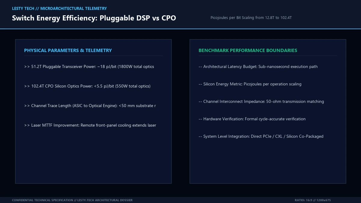
To overcome 35 dB of attenuation, the switch ASIC’s physical layer (SerDes) must employ massive Continuous-Time Linear Equalization (CTLE), multi-tap Feed-Forward Equalization (FFE), and high-order Decision Feedback Equalization (DFE). At 102.4 Tbps (requiring 512 lanes of 224 Gbps SerDes), the electrical PHY alone consumes over 1,800 Watts of electrical power, operating at ~18 to 22 picojoules per bit (pJ/bit).
Co-Packaged Optics radically transforms this topology. By placing silicon photonic optical engines directly on the multichip package substrate adjacent to the switch ASIC, electrical trace reach is compressed from 18 inches down to under 30 to 50 millimeters. With trace loss dropping to less than 3 dB, the complex DSP equalizers can be completely eliminated or replaced with ultra-lightweight linear analog drivers (Direct-Drive / Linear Pluggable Optics architecture), slashing SerDes power to under 1.5 pJ/bit.
2. The Thermal Physics of Laser Degradation: Why On-Die Lasers Fail
If co-packaging optical engines onto the compute substrate is so advantageous, why not integrate the laser light sources directly into the silicon photonic die using heterogeneous III-V/Silicon epitaxial bonding?
The answer lies in the unforgiving solid-state physics of semiconductor laser diodes: Indium Phosphide (InP) Distributed Feedback (DFB) lasers are catastrophically sensitive to operating temperature.
A continuous-wave (CW) DFB laser diode generates coherent optical power through the radiative recombination of injected carriers in quantum wells. As junction temperature (Tj) increases, non-radiative Auger recombination scales exponentially, and carrier leakage out of the active quantum wells accelerates according to the Arrhenius relation:
Where Ith is the threshold current, T0 is the characteristic temperature parameter (typically 50K to 70K for InP lasers), and \(\eta_{\text{slope}}\) is the differential quantum efficiency.
In a 102.4 Tbps switch, the core ASIC dissipates between 800W and 1,200W of heat across a package area of just 100 × 100 mm. Operating under heavy AI all-reduce collective communications, substrate temperatures consistently hover between 85°C and 105°C.
Placing an InP laser directly on this substrate incurs three catastrophic engineering penalties:
- Optical Power Collapse: At 95°C, laser threshold current quadruples while slope efficiency collapses by >65%. To maintain a mandatory +17 dBm (50 mW) continuous optical output per channel, the laser must be driven with extreme forward current, precipitating instantaneous thermal runaway.
- Accelerated MTTF Aging: Laser diode operating lifetime follows Black’s Equation and Arrhenius degradation kinetics: \(\text{MTTF} \propto \exp\left( \frac{E_a}{k_B T_j} \right)\), where activation energy \(E_a \approx 0.7 \text{ eV}\). Operating a laser at 95°C degrades its operating lifetime by a factor of over 25x compared to operating at 45°C, reducing Mean Time To Failure from 15 years down to less than 7 months!
- Unserviceable Board Scrapping: In a heterogeneous CPO switch with 64 on-package laser diodes, the failure of a single non-replaceable laser diode permanently disables the entire optical engine, forcing data center operators to scrap a \$120,000+ switch chassis.
3. The OIF-ELSFP Architecture: Remote Laser Decoupling
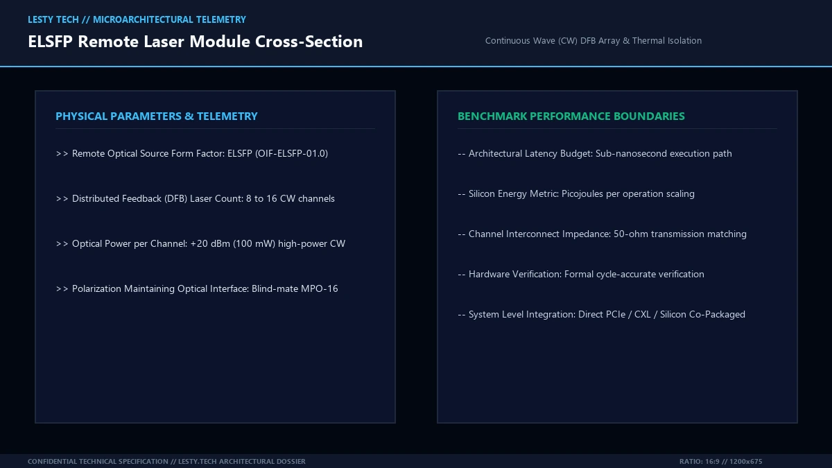
To resolve the laser thermal paradox, the Optical Internetworking Forum (OIF) established the External Laser Small Form-Factor Pluggable (ELSFP) specification (OIF-ELSFP-01.0).
The architectural breakthrough of the copackaged optics elsfp laser is the complete physical decoupling of photon generation from photon modulation:
- The Core CPO Substrate: Houses only passive silicon photonic Mach-Zehnder Modulators (MZMs), micro-ring resonators, and germanium photodetectors integrated alongside the switch ASIC. Silicon photonics is composed of robust silicon-on-insulator (SOI) crystals that operate flawlessly at 105°C without aging degradation.
- The ELSFP Remote Module: Houses the delicate continuous-wave InP DFB laser arrays located on the cool, front-panel chassis faceplate. Cooled by incoming ambient data center air (25°C to 35°C) and equipped with internal thermoelectric coolers (TEC), the lasers operate in an ideal thermal environment (\(T_j \approx 45^\circ\text{C}\)), guaranteeing multi-decade operating reliability.
| Architectural Metric | OIF ELSFP Remote Laser | On-Package Heterogeneous III-V | Pluggable OSFP-XD Transceiver |
|---|---|---|---|
| Laser Junction Temp (Tj) | 40°C – 50°C (Front Panel) | 85°C – 105°C (ASIC Heat) | 65°C – 75°C (Enclosed Module) |
| Laser MTTF Reliability | >10,000,000 Hours | <450,000 Hours | ~2,500,000 Hours |
| Field Serviceability | Hot-Swappable in 5 Seconds | Non-Serviceable (Board Scrap) | Hot-Swappable Module |
| Total Switch Electro-Optic Power | <5.2 pJ / bit | 4.8 pJ / bit | 18.5 – 22.0 pJ / bit |
| Optical Interconnect Interface | PMF MPO-16 Blind-Mate | Direct Waveguide Coupler | Front LC / MPO Receptacle |
An ELSFP module packages an array of 8 to 16 unmodulated high-power CW DFB laser channels. Each channel emits between +17 dBm (50 mW) and +20 dBm (100 mW) of pure optical power at standardized telecom wavelengths (typically CWDM4 grids around 1310 nm).
If an ELSFP laser module experiences degradation over time, data center telemetry detects the optical power dropoff. A technician simply hot-swaps the faulty ELSFP module on the front panel in seconds without powering down the switch ASIC, disrupting network routing, or breaking the vacuum of the co-packaged multichip module.
4. Optical Interconnect Engineering: Polarization-Maintaining Fiber (PMF)
While remote laser placement solves the thermal crisis, it introduces a demanding optical physics challenge: Polarization Extinction Ratio (PER) Maintenance.
Silicon photonic modulators (both Mach-Zehnder and micro-ring topologies) are fundamentally polarization-sensitive. Waveguide sub-micron cross-sections (\(450 \text{ nm} \times 220 \text{ nm}\)) exhibit extreme geometric birefringence: they support only the Transverse Electric (TE) fundamental mode. If light enters the optical engine with Transverse Magnetic (TM) polarization, modulation efficiency collapses and insertion loss exceeds 20 dB.
Guiding light from the front-panel ELSFP module to the on-package optical engine requires specialized Polarization-Maintaining Fiber (PMF) ribbons:
PMF fibers incorporate internal stress-applying elements (such as PANDA or bow-tie stress rods) that induce strong artificial birefringence. Light polarized along the slow axis is trapped by the phase mismatch, preventing energy coupling into the fast axis even when the fiber undergoes mechanical bending inside the switch chassis.
Furthermore, connecting the ELSFP module to internal fiber routing requires blind-mate optical connectors (such as blind-mate MPO-16 or MXC connectors). These connectors utilize high-precision ceramic alignment guide pins and physical contact angled polish (APC 8°) to guarantee:
- Insertion loss strictly below 0.3 dB per interface.
- Optical return loss (ORL) exceeding 55 dB to prevent back-reflections from destabilizing DFB laser oscillation modes.
- Polarization axis angular alignment tolerance tighter than ±1.5 degrees.
4.1. Silicon Photonic Modulators: Micro-Rings vs. Mach-Zehnder Interferometers
Once the continuous optical carrier beam arrives at the on-package optical engine, the continuous wave (CW) photons must be modulated with the high-speed 224 Gbps electrical data stream. Modern CPO architectures deploy two distinct electro-optic modulator topologies:
- Traveling-Wave Mach-Zehnder Modulators (MZM): MZMs split the optical carrier into two balanced interferometer arms, applying differential phase shifts via the plasma dispersion effect in reverse-biased PN junctions. While MZMs deliver exceptional optical bandwidth and thermal stability over a broad wavelength range (10 nm to 20 nm optical window), they occupy substantial silicon area (lengths of 1.5 to 3.0 mm) and demand higher capacitive drive power (\(V_\pi \cdot L \approx 1.2 \text{ to } 1.8 \text{ V}\cdot\text{cm}\)).
- Micro-Ring Resonators (MRR): Micro-rings couple light into an ultra-compact circular waveguide ring (diameter of 5 to 10 micrometers). By modulating the refractive index through carrier injection, the ring’s sharp Lorentzian resonance peak shifts in and out of alignment with the laser wavelength. MRRs feature a microscopic silicon footprint (100x smaller than MZMs) and consume under 50 fJ/bit of modulation energy. However, micro-rings have a narrow Free Spectral Range (FSR) and are acutely sensitive to localized temperature drift (\(\approx 0.1 \text{ nm/}^\circ\text{C}\)), requiring active micro-heater closed-loop feedback circuits to lock resonance to the incoming ELSFP carrier.
4.2. Laser Eye Safety and Automatic Power Shutdown (APSD)
An ELSFP module concentrates between +17 dBm and +23 dBm (up to 200 mW) of raw continuous-wave laser power into a multi-core fiber ribbon. Under OSHA and IEC 60825-1 laser safety regulations, exposing an unshielded fiber carrying this intensity into free space represents an extreme Class 3B/Class 4 ocular hazard that can cause instant, permanent retinal blindness.
To satisfy Class 1M eye safety certification, ELSFP systems implement Automatic Power Shutdown (APSD) and Optical Loss of Signal (LOS) interlock loops. The module incorporates physical micro-switches and electrical sense pins on the blind-mate connector. If an ELSFP module is unlatched or an internal fiber ribbon is severed, the hardware interlock loop breaks, triggering microcode registers to extinguish all CW laser outputs in under 10 milliseconds—long before an operator can withdraw the module from the chassis faceplate.
Co-Packaged Optics Laser Subsystems: ELSFP vs. Heterogeneous III-V
Continuous Wave Laser Reliability, Polarization Maintaining Interconnects, and 102.4T Switch Architectures (Complete architectural audit with telemetry tables and schematic breakdowns).
whitepaper_batch_17_4_copackaged_optics_elsfp.pdfFormat: Publication-Grade PDF
5. Datacenter TCO: 102.4T Power Budget and Economic Analysis
The economic imperative driving the deployment of the copackaged optics elsfp laser architecture is total cost of ownership (TCO) and datacenter electrical facility limits.
In a mega-datacenter housing 1,000 top-of-rack switches operating at 102.4 Tbps:
- Traditional Pluggable Switch Fabric: 1,000 switches × 2,800 Watts per switch = 2.80 Megawatts of power dedicated purely to networking. At an average enterprise electricity cost of \$0.10/kWh, powering and cooling this network consumes \$4.9 million annually.
- CPO Fabric with ELSFP Remote Lasers: 1,000 switches × 1,150 Watts per switch = 1.15 Megawatts of power. Annual electrical operating costs plummet to \$2.0 million, generating \$2.9 million in annual power savings alone.
More importantly, freeing up 1.65 Megawatts of facility power within an existing power-constrained datacenter envelope allows hyperscalers to deploy an additional 1,600 high-performance AI accelerator GPUs without expanding physical building square footage.
6. Frequently Asked Questions (FAQ)
What is the primary difference between a standard pluggable transceiver and an ELSFP module?
A standard pluggable transceiver (such as an OSFP or QSFP-DD) contains a complete electro-optic transmission system: high-speed DSP re-timers, laser transmitters, optical modulators, and photodetector receivers. An ELSFP (External Laser Small Form-Factor Pluggable) module contains only unmodulated continuous-wave (CW) laser diodes and thermoelectric coolers. Modulation and optical detection take place directly on the compute substrate inside the switch’s co-packaged optical engines.
Why can’t silicon itself emit laser light?
Silicon is an indirect bandgap semiconductor: the conduction band minimum and valence band maximum occur at different crystal momentum vectors. When an electron recombines with a hole in silicon, it requires phonon mediation (lattice vibration), resulting in non-radiative thermal recombination rather than photon emission. Efficient semiconductor lasers require direct bandgap III-V compound semiconductors like Indium Phosphide (InP) or Gallium Arsenide (GaAs).
How many optical fibers connect an ELSFP module to the CPO switch package?
An ELSFP module typically connects via an internal polarization-maintaining fiber (PMF) ribbon containing 8 or 16 fibers. Each fiber feeds a continuous optical carrier beam into an on-package optical engine, where it is split or routed into multiple silicon photonic modulators.
Is CPO with ELSFP backwards compatible with existing datacenter fiber infrastructure?
Yes. The internal connection between the ELSFP and the CPO optical engine is purely internal to the switch chassis. The output ports on the front panel that connect to the external datacenter fabric utilize standard single-mode optical fiber (SMF) terminating in industry-standard MPO-16, SN, or MDC connectors, matching existing structured fiber cabling.
7. Architectural Conclusion: The Optical Foundation of 102.4T Networks
The transition to 102.4 Tbps network switching represents the physical inflection point where pure copper electrical interconnects must yield to integrated photonics. While heterogeneous on-package laser integration presented an alluring theoretical vision, the harsh thermal realities of semiconductor physics and datacenter serviceability rendered it unviable for mission-critical infrastructure.
The copackaged optics elsfp laser architecture delivers the optimal engineering balance: compressing high-loss copper SerDes traces to millimetric scales on the multichip substrate while isolating delicate high-power laser diodes in a cool, field-serviceable front-panel envelope. By slashing network energy consumption below 5.5 pJ/bit, preserving high laser MTTF reliability, and maintaining full compatibility with enterprise maintenance workflows, ELSFP co-packaged optics provides the foundational physical layer that will power the next decade of hyperscale AI supercomputing.
Related Technical Dossiers & Internal Research
- UCIe 2.0 Die-to-Die Interconnects: Physical Layer (PHY), 2.5D Packaging, and Sub-Nanosecond Latency Physics →
- Diamond Heat Spreaders & Heterogeneous GaN Integration: The Phonon Transport Physics Dissipating 2,000 W/cm² →
- Photonic Tensor Processors & Mach-Zehnder Interferometers: The Silicon Light Waveguide Physics Slashing AI MatMul Energy →
Authoritative External Reference
Reference Citation: OIF (Optical Internetworking Forum): Co-Packaged Optics (CPO) and ELSFP Module Implementation Agreement →