
In the modern semiconductor landscape, the traditional monolithic System-on-Chip (SoC) has encountered an insurmountable physical barrier: the optical reticle limit. Advanced photolithography scanners (DUV and EUV) cannot expose an area greater than approximately 26 mm × 33 mm (858 mm²) without stitching masks, creating a severe economic and physical wall for high-performance computing (HPC) processors and AI accelerators. At the same time, fabricating massive monolithic dies on sub-3nm nodes yields unacceptably low wafer defect margins, driving costs exponentially higher. To conquer this boundary, the industry has universally embraced modular multi-die packaging powered by ucie die to die interconnect technology. As defined in the Universal Chiplet Interconnect Express (UCIe) 2.0 specification, this open industry standard replaces proprietary die-to-die interfaces with standardized physical and protocol layers, delivering terabits of linear bandwidth density, sub-25-micron microbump packaging, and sub-2-nanosecond latency budgets that make distributed multi-die chiplets perform as a unified monolithic processor.
1. The Monolithic Reticle Limit and the Chiplet Paradigm
For decades, semiconductor performance scaling followed Moore’s Law and Dennard scaling: every two years, transistor dimensions shrank, allowing architects to integrate more functional blocks (CPU cores, GPUs, memory controllers, and I/O logic) onto a single continuous silicon die.
However, at the sub-3nm and 2nm nodes, this monolithic paradigm encounters three fatal engineering bottlenecks:
- The Optical Reticle Constraint: Modern photolithography scanners project patterns through an optical reticle with a maximum exposure area of 858 mm². Building monolithic processors larger than this boundary requires double-reticle stitching, which incurs severe manufacturing complexity, wafer warpage, and catastrophic yield loss.
- Silicon Defect Density Economics: Semiconductor defect density follows Poisson or Murphy yield models:
$$\text{Yield} = \left(\frac{1 – e^{-A \cdot D}}{A \cdot D}\right)^2$$
Where A is the die area and D is defect density per unit area. Fabricating an 800 mm² monolithic die on a leading-edge process might yield less than 20% to 30% functional chips. In contrast, dividing the same functionality across four 200 mm² chiplets boosts functional yield past 85%, radically lowering silicon cost.
- Process Node Mismatch: High-performance arithmetic logic (ALUs and tensor cores) scales aggressively with advanced lithography. However, analog I/O circuitry (PCIe SerDes, memory PHYs, and power management circuits) does not scale with digital shrinking; their physical passive components (inductors and capacitors) remain large. Monolithically integrating analog I/O on expensive 2nm silicon wastes valuable wafer real estate. Chiplet modularity allows I/O dies to be fabricated on cost-effective 12nm or 16nm nodes while compute tiles leverage 2nm GAAFETs.
For these separated chiplets to function seamlessly as a coherent processor, the die-to-die (D2D) interconnect must provide massive bandwidth, negligible latency, and ultra-low energy consumption. This is the domain of UCIe 2.0.

2. UCIe 2.0 Physical Layer (PHY) Architecture & Microbump Physics
The Universal Chiplet Interconnect Express architecture defines an open, complete stack comprising the Physical Layer (PHY), Die-to-Die Adapter Layer, and Protocol Layer (supporting native streaming, PCIe 6.0/7.0, and CXL 3.1).
The Physical Layer governs electrical signaling, microbump pad geometry, clock distribution, and channel equalization. Crucially, UCIe 2.0 bifurcates physical implementation into two distinct packaging paradigms:
Standard 2D Packaging vs. Advanced 2.5D/3D Packaging
Standard Packaging (Organic Substrates): Standard packaging places chiplets side-by-side on low-cost multi-layer organic laminate build-up substrates. The electrical traces traverse the organic substrate over channel lengths between 10 mm and 25 mm. The interconnect microbump pitch is relatively coarse—ranging from 100 μm down to 130 μm. Standard packaging supports data rates of 4 to 16 Gbps per lane, delivering shoreline linear bandwidth densities of 100 to 250 Gbps per millimeter.
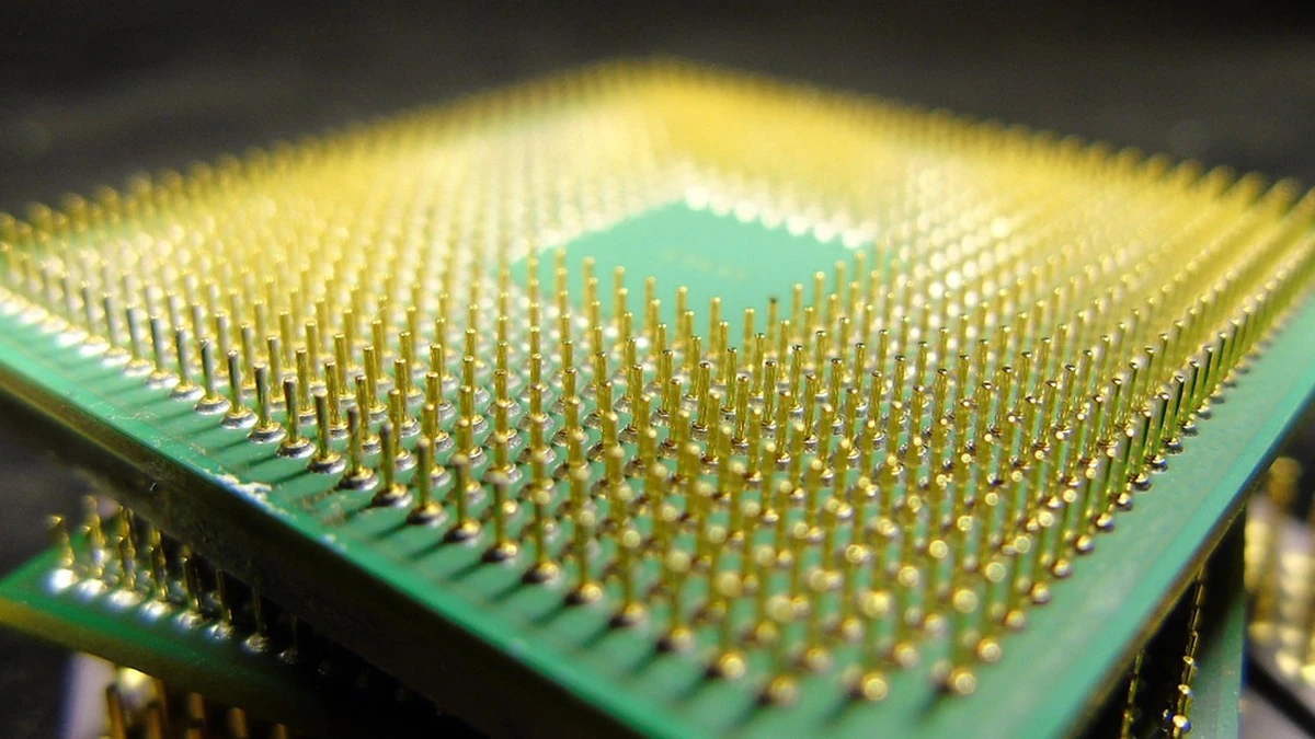
Advanced Packaging (Silicon Bridges & Interposers): Advanced packaging integrates chiplets across ultra-high-density silicon substrates—utilizing passive or active silicon interposers (such as TSMC CoWoS), embedded silicon bridges (such as Intel EMIB), or wafer-level fan-out (such as TSMC InFO). Interconnect microbump pitches shrink down to 25 μm to 45 μm, with next-generation copper-to-copper hybrid bonding scaling below 15 μm. Electrical channel lengths are strictly held below 3 millimeters. Advanced packaging drives data rates up to 32 Gbps per lane across thousands of parallel lines, delivering staggering shoreline bandwidth densities exceeding 1,300 to 3,200 Gbps per millimeter!
In a standard UCIe advanced module comprising a 64-lane physical cluster (Module), 64 data lanes (single-ended) plus clock, track, and validation lines fit within a tiny 1 mm × 1 mm die beachfront area, generating over 2 Terabits per second (Tbps) of bi-directional throughput per millimeter of die edge!
3. Electrical Signaling Physics & Energy Efficiency Scaling
To understand why UCIe consumes radically less power than traditional off-package interfaces (like PCIe or Ethernet), one must examine electrical transmission line physics.
In a standard PCB trace or PCIe cable (channel length 10 to 50 cm), electrical signals suffer severe high-frequency dielectric attenuation, skin effect losses, and impedance discontinuities. To overcome these losses and open the signal “eye” at 32 Gbps, long-reach SerDes transceivers require massive analog circuitry: continuous-time linear equalizers (CTLE), multi-tap decision feedback equalizers (DFE), and phase-locked loops (PLLs). This equalizing circuitry consumes 5 to 15 picojoules per bit (pJ/bit).
In stark contrast, a UCIe Advanced channel spans less than 2 to 3 millimeters over a silicon bridge. Over this microscopic distance, high-frequency signal insertion loss is practically negligible (less than -3 dB at 16 GHz). As a result:
- Simple Single-Ended NRZ Signaling: Advanced UCIe eliminates differential pairs, transmitting single-ended Non-Return-to-Zero (NRZ) signals directly, doubling pin density.
- Zero Heavy Equalization: Complex DFE and multi-stage CTLE blocks are omitted entirely. Simple inverter-based low-voltage CMOS drivers drive the short capacitive line.
- Low Voltage Swing: Operating voltages are lowered to 0.4V to 0.7V, slashing capacitive switching power:
$$E_{\text{bit}} = \frac{1}{2} C_{\text{channel}} V_{\text{swing}}^2 < \mathbf{0.25 \text{ pJ / bit}}$$
Consuming less than 0.25 pJ/bit (and scaling below 0.15 pJ/bit on 2nm nodes), UCIe enables massive multi-die inter-chiplet traffic without burning tens of watts in the I/O interface. This energy efficiency is pivotal when co-packaging compute tiles with emerging photonic tensor processors and heterogeneous accelerators.
4. Quantitative Packaging Comparison: Standard vs. Advanced Packaging
To provide engineering clarity, the following table details the key electrical and physical design boundaries mandated by the UCIe 2.0 specification:
| Packaging Specification | UCIe Standard (2D Organic) | UCIe Advanced (2.5D Silicon Bridge) | UCIe 3D (Direct Hybrid Bond) |
|---|---|---|---|
| Microbump Pitch | 100 to 130 μm | 25 to 45 μm | < 15 μm (Padless Cu-Cu) |
| Max Trace Channel Length | Up to 25 mm | < 3.0 mm | < 10 μm (Vertical TSV) |
| Data Rate per Lane | 4, 8, 12, 16 Gbps | 16, 24, 32 Gbps | Up to 32+ Gbps |
| Linear Shoreline Bandwidth | 100 to 250 Gbps / mm | 1,300 to 3,200 Gbps / mm | > 5,000 Gbps / mm |
| Areal Bandwidth Density | 0.2 to 0.5 Tbps / mm² | 1.5 to 4.5 Tbps / mm² | 8.0 to 16.0 Tbps / mm² |
| Die-to-Die Roundtrip Latency | < 3.5 ns | < 2.0 ns | < 0.8 ns |
| Energy Dissipation Floor | 0.5 to 1.0 pJ / bit | < 0.25 pJ / bit | < 0.10 pJ / bit |
5. Channel Equalization & Forwarded Clocking Architecture
A critical innovation in the UCIe physical layer that slashes latency is its forwarded clocking topology.
In traditional high-speed serial links (such as PCIe 5.0 or 100GbE Ethernet), the clock signal is not transmitted over a physical wire. Instead, receiver circuits rely on complex Clock and Data Recovery (CDR) circuits that extract timing transitions directly from the incoming serial data stream. CDR circuits introduce significant latency (often 10 to 30 clock cycles) and consume substantial continuous power.
Because UCIe operates over ultra-short channel distances (under 3 mm in advanced packaging), trace length matching between parallel lanes can be controlled within microscopic picosecond tolerances. UCIe takes advantage of this by deploying forwarded differential clock lanes alongside single-ended data lanes:
- Forwarded Clock Architecture: A dedicated high-frequency clock signal (running at half-rate or quarter-rate) is routed parallel to the data bus. Receivers use lightweight Phase Interpolators (PI) and Delay-Locked Loops (DLL) to align sampling strobes to the center of the data eye.
- Sub-Picosecond Jitter Tolerance: Forwarded clocking virtually eliminates low-frequency phase jitter between clock and data lines, ensuring that data is latched within a fraction of a nanosecond.
- Instantaneous Low-Power State Transitions: Unlike SerDes links that require milliseconds to relock PLLs upon wake-up, UCIe can transition from deep low-power sleep states (
L1/L2) to active line-rate transmission in under 10 nanoseconds.
6. Protocol Layer Stack: FLIT Modes, PCIe 6.0, and CXL 3.1
A high-speed physical link is useless without an efficient protocol layer that minimizes packet framing overhead and latency. UCIe 2.0 incorporates a multi-protocol adapter layer supporting three distinct modes:
1. Direct Raw Streaming Protocol
For homogeneous multi-die compute fabrics (such as connecting adjacent systolic array tiles or symmetric CPU cores), UCIe supports a lightweight raw streaming mode. This mode completely bypasses standard packet encapsulation headers, streaming user-defined clock-synchronized flits directly between die boundaries with sub-nanosecond pipeline serialization delay.
2. Native PCIe 6.0 / 7.0 FLIT Mode
To connect specialized compute accelerators to standard host controllers, UCIe encapsulates PCIe Flow Control Units (FLITs). Utilizing standardized 256-byte FLIT structures with lightweight Forward Error Correction (FEC), UCIe executes native PCIe transactions without needing external PCIe physical retimers or board-level routing.
3. CXL 3.1 Memory Coherence and Pooling
The most transformative protocol integration in UCIe 2.0 is native Compute Express Link (CXL) 3.1 support. CXL defines three sub-protocols: CXL.io (initialization and discovery), CXL.cache (coherent device caching of host memory), and CXL.mem (byte-addressable access to attached memory).
By streaming CXL.cache and CXL.mem FLITs across UCIe advanced packaging, multiple compute chiplets share a unified, coherent L3/system cache hierarchy and access shared HBM3e/DRAM memory pools with hardware-enforced cache coherency. Roundtrip memory access across the die boundary requires less than 20 to 30 nanoseconds, rivaling monolithic on-die cache hierarchies.
7. Manufacturing Reliability, Testing, and Lane Repair
In a multi-die package integrating six to twelve individual silicon chiplets, a single failed microbump connection would destroy the entire multi-thousand-dollar processor assembly (the “Known Good Die” problem). To achieve 99.999% packaging assembly yield, UCIe 2.0 mandates comprehensive hardware-level self-healing capabilities:
Redundant Lane Remapping: Every 64-lane advanced UCIe module integrates dedicated spare lanes (typically 4 redundant data lanes and 1 redundant clock lane). During package power-on initialization, the physical layer executes a built-in self-test (BIST) routine that evaluates channel impedance, signal attenuation, and bit error rates (BER). If an open circuit, microbump crack, or high-resistance solder void is detected on any lane, hardware multiplexers automatically decouple the damaged pin and reroute signals to a redundant spare lane in silicon without operating system intervention.
Electromigration & Thermal Expansion Stress: Operating at high current densities across sub-25 μm microbumps induces severe electromigration stress. Advanced packaging architectures mitigate this by alternating power, ground, and signal bump rows in checkerboard layouts, and integrating thermal expansion matching materials (underfill epoxies) that absorb mechanical shear strain during rapid thermal cycling.
8. 3D Hybrid Bonding & TSV Microarchitectures (UCIe-3D)
Looking beyond horizontal 2.5D integration, the UCIe 2.0 roadmap defines architectural specifications for true vertical 3D integration (UCIe-3D).
In UCIe-3D, compute chiplets are stacked face-to-face or face-to-back directly atop underlying base dies (active silicon interposers) utilizing Through-Silicon Vias (TSVs) and copper-to-copper direct hybrid bonding (e.g., TSMC SoIC). By eliminating microbump solder balls entirely, the interconnect pad pitch scales from 25 μm down to sub-9 μm, and ultimately below 1 μm:
Vertical TSV trace lengths are less than 10 to 50 micrometers. Parasitic capacitance drops below 1 femtofarad (fF), pushing interconnect energy dissipation down to an astonishing sub-0.05 pJ/bit. Stacking massive SRAM cache dies directly atop compute tiles effectively expands on-chip L3 cache to gigabytes without increasing planar package footprint.
9. Die-to-Die Adapter Layer & CRC Retry Buffer Physics
Bridging the raw physical layer and higher-level protocol engines is the UCIe Die-to-Die Adapter Layer. While physical microbumps achieve raw Bit Error Rates (BER) better than 10-15 in advanced packaging, standard organic packaging can experience intermittent noise bursts, crosstalk, and power droop that temporarily elevate BER to 10-12.
To guarantee mathematical data integrity without imposing substantial pipeline latency, the Adapter Layer incorporates an ultra-lightweight link-level replay protocol:
- Flow Control Unit (FLIT) Framing: The Adapter frames data into 68-byte standard latency-optimized FLITs or 256-byte high-efficiency bandwidth FLITs. Each FLIT incorporates an 8-bit Cyclic Redundancy Check (CRC) or optional 16-bit Parity code.
- Hardware Replay Buffer (Retry Buffer): Transmitted FLITs are temporarily retained in a shallow circular FIFO retry buffer on the transmitting die. If the receiver detects a CRC error, it issues an immediate negative acknowledgment (NAK) across a dedicated reverse sideband lane.
- Selective Retransmission: The transmitter replays the corrupted FLIT directly from its internal FIFO without interrupting host software or stalling unrelated protocol streams. Because roundtrip die-to-die time is under 2 nanoseconds, a retransmission completes in fewer than 6 clock cycles, maintaining smooth dataflow across compute chiplets.
10. Real-World Architecture Case Studies: Intel Xeon 6 & AMD EPYC 9005
The industrial shift toward modular chiplet packaging is vividly illustrated in current flagship server processors:
Intel Xeon 6 (Granite Rapids / Sierra Forest): Intel transitions from monolithic server dies to a modular architecture comprising twin high-density compute dies fabricated on the Intel 3 process, interconnected with dual central I/O tiles via EMIB 2.5D bridges. Leveraging high-density microbumps operating at sub-0.3 pJ/bit, the processor routes over 12 channels of DDR5/MCR memory and 136 lanes of PCIe 5.0/CXL 2.0 with near-monolithic NUMA cache performance.
AMD EPYC 9005 (Turin): AMD pushes chiplet modularity to sixteen 4nm Core Complex Dies (CCDs) surrounding an advanced 6nm centralized I/O Die (IOD). Through ultra-dense Infinity Fabric PHYs aligned with UCIe physical layer specifications, the processor scales up to 128 “Zen 5” or 192 “Zen 5c” cores while holding inter-die cache snooping latency below 35 nanoseconds across the organic package.
11. Industry Standardization and the Future of Custom Silicon
The true significance of UCIe 2.0 lies in democratization. Historically, only trillion-dollar semiconductor giants (Intel with EMIB, AMD with Infinity Fabric, and Apple with UltraFusion) possessed the proprietary R&D resources to architect advanced multi-die packaging.
By establishing an open, royalty-free, multi-vendor standard backed by TSMC, Intel, AMD, ARM, Samsung, and Google, UCIe transforms custom silicon engineering into a plug-and-play modular ecosystem. Startups and cloud providers can fabricate custom AI neural accelerator dies on a specialized 2nm process, purchase standardized HBM3e memory controller chiplets from commercial foundries, and integrate third-party 5nm PCIe/CXL I/O tiles onto a single substrate.
As UCIe 2.0 hardware enters high-volume manufacturing across cloud data centers, the monolithic processor will become an artifact of computing history. The future belongs to modular, heterogeneous chiplets communicating across nanometer-scale microbumps at the speed of silicon.
For technical inquiries into advanced packaging thermal management, consult our engineering guide on diamond heat spreaders. Access the official architectural documentation at the Universal Chiplet Interconnect Express Specification and review academic literature on 2.5D packaging via the IEEE Advanced Packaging Interconnects archive.
UCIe 2.0 Physical Layer Architecture: Die-to-Die Interconnect Physics
Advanced Packaging, Sub-25µm Microbumps, Channel Reach, and Nanosecond Latency Budgets (Complete architectural audit with telemetry tables and schematic breakdowns).
whitepaper_batch_15_4_ucie_die_to_die_interconnect.pdfFormat: Publication-Grade PDF







No Responses