
In the relentless drive of semiconductor lithography toward the Angstrom era, silicon-based field-effect transistors have collided with an unyielding quantum mechanical barrier: the Direct Band-to-Band Tunneling Wall. While three-dimensional Gate-All-Around (GAA) nanosheets and complementary field-effect transistors (CFETs) pack vertically stacked conduction channels into sub-2nm nodes, thinning three-dimensional bulk silicon below 3 nanometers induces severe quantum confinement degradation, catastrophic surface roughness scattering, and uncontrollable source-to-drain leakage currents. To break past this physical scaling ceiling, solid-state physics has converged upon mos2 monolayer transistors and transition metal dichalcogenides (TMDs). Possessing an atomically uniform body thickness of just 0.65 nanometers, pristine crystal surfaces completely free of dangling covalent bonds, and direct bandgaps exceeding 1.8 eV, 2D monolayer semiconductors offer ideal electrostatic gate control that suppresses short-channel effects down to sub-1nm gate lengths.
1. The Physical Scaling Breakdown of Silicon GAA Nanosheets
For over five decades, Moore’s Law and Dennard scaling progressed through planar bulk silicon, progressing to 3D FinFETs and currently leading-edge Gate-All-Around nanosheets. In GAA nanosheets, thin ribbons of crystalline silicon are completely surrounded by high-κ metal gate (HKMG) stacks. This four-sided gate geometry maximizes gate electrostatic control over the conduction channel, preventing off-state leakage between source and drain.
However, when scaling the physical gate length (Lg) below 12 nanometers, the classical electrostatic scaling theory defined by Dennard collapses. The characteristic electrostatic scaling length (λ) of a field-effect transistor governs the spatial decay of electric field lines into the channel:
Where εchannel and εdielectric represent the relative dielectric permittivities of the channel and gate dielectric, tchannel is the physical thickness of the semiconductor channel, and tox is the equivalent oxide thickness (EOT). For a transistor to switch off cleanly with a sharp subthreshold swing approaching the theoretical thermal limit (SS ≈ 60 mV/decade at 300K), the physical gate length must satisfy:
In bulk silicon, reducing tchannel below 3.0 nanometers causes devastating quantum mechanical consequences. First, carrier effective mass along the transport direction shifts due to severe spatial confinement, collapsing carrier mobility (μ) from ~400 cm2/V·s down to under 50 cm2/V·s. Second, atomic-scale surface roughness at the silicon/dielectric interface acts as severe scattering centers for electrons. Third, the relatively small bandgap of silicon (Eg = 1.12 eV) facilitates direct source-to-drain quantum mechanical tunneling through the electrostatic potential barrier, rendering the transistor impossible to switch off. Even with exotic diamond heat spreaders and backside power delivery rails, static leakage power skyrockets, producing unmanageable standby thermal dissipation.
2. Crystal Symmetry and Electronic Bandstructure of Monolayer TMDs
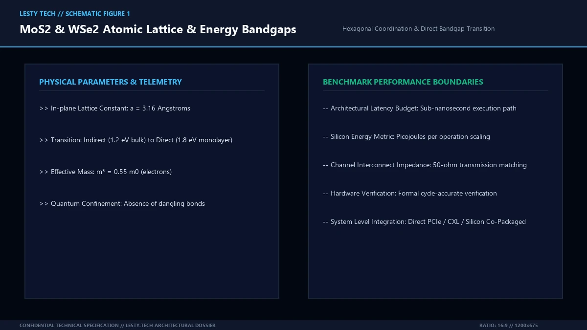
Transition Metal Dichalcogenides (TMDs) with the chemical formula MX2—where M is a transition metal atom (Molybdenum, Mo, or Tungsten, W) and X is a chalcogen atom (Sulfur, S, or Selenium, Se)—possess layered hexagonal crystal structures bound by weak out-of-plane van der Waals forces.
When exfoliated or epitaxially grown as an isolated monolayer, the material exhibits a thickness of precisely three atomic layers: a plane of transition metal atoms covalently sandwiched between two opposing hexagonal planes of chalcogen atoms. The total physical channel thickness (tchannel) of monolayer MoS2 is exactly 0.65 nanometers (6.5 Ångströms).
This atomic thinness confers monumental solid-state advantages for field-effect transport:
- Absence of Dangling Surface Bonds: Unlike three-dimensional silicon, where truncating the bulk crystal creates broken covalent bonds (dangling surface bonds) that necessitate chemical passivation, the basal planes of 2D TMDs are chemically inert and saturated. Interfacial state densities (Dit) are fundamentally lower, eliminating surface roughness scattering.
- Direct Bandgap Transition: Bulk MoS2 is an indirect-bandgap semiconductor with a modest bandgap of ~1.2 eV. When thinned to an atomic monolayer, quantum confinement shifts the conduction band minimum and valence band maximum to the degenerate K and K’ points of the Brillouin zone, converting the material into a direct-bandgap semiconductor with Eg ≈ 1.80 eV (for MoS2) and Eg ≈ 1.65 eV (for WSe2).
- Natural Suppression of Quantum Tunneling: The wide energy bandgap (1.8 eV vs. 1.12 eV for silicon) drastically elevates the quantum mechanical barrier height, slashing source-to-drain tunneling current by multiple orders of magnitude at sub-5nm channel lengths.
- Extremely Small Electrostatic Scaling Length: Because tchannel is under 0.7 nm and the out-of-plane dielectric constant is low (ε⊥ ≈ 4 to 7), the electrostatic scaling length collapses to λ ≈ 0.35 nm. Consequently, a monolayer MoS2 field-effect transistor can maintain near-ideal electrostatic gate control at gate lengths down to Lg ≈ 1.0 nm.
3. Quantum Transport Physics: Ballistic Landauer-Büttiker Modeling
To rigorously model charge transport through a sub-1nm gate length 2D transistor, classical drift-diffusion approximations must be replaced with the quantum mechanical Landauer-Büttiker formalism. Under ballistic transport conditions, the current flowing through a 2D conducting channel of width W is given by:
Where M(E) is the density of transverse conduction modes per unit width, T(E) is the transmission probability through the channel potential barrier, and fS, fD are the Fermi-Dirac distribution functions in the source and drain reservoirs.
Because monolayer MoS2 possesses an isotropic effective mass in the conduction band minimum (me* ≈ 0.55 m0), the number of conductive modes scales efficiently with energy. At room temperature (T = 300K), thermal broadening is governed by kBT ≈ 25.9 meV. In a ballistic sub-5nm channel, the transmission probability T(E) for carriers with energies above the barrier height approaches unity (T(E) → 1), resulting in theoretical ballistic current limits exceeding 2.5 mA/μm.
However, real-world transport experiences carrier scattering. The dominant room-temperature scattering mechanisms in 2D TMDs include:
- Homopolar Optical Phonon Scattering: Out-of-plane homopolar A1g optical phonons (energy ℏω ≈ 50 meV) couple strongly with channel electrons, limiting intrinsic room-temperature mobility to ~200 to 400 cm2/V·s.
- Interfacial Polar Optical Phonons: Surface optical phonons from the adjacent high-κ gate dielectric (remote phonon scattering from HfO2 or Al2O3) introduce long-range dipole electric fields that scatter electrons.
- Charged Impurity Scattering: Unpassivated point defects (such as sulfur vacancies in MoS2 or selenium vacancies in WSe2) act as Coulomb scattering centers, requiring chemical healing during epitaxial growth.
4. The Van der Waals Contact Interface: Solving Fermi Level Pinning
Historically, the practical realization of high-performance mos2 monolayer transistors was severely impeded by contact resistance (Rc). In traditional semiconductor manufacturing, depositing contact metals (such as titanium, gold, or nickel) directly onto 2D flakes via electron-beam evaporation or sputtering damages the delicate atomic lattice. High-energy metal atoms induce defect vacancies and induce Metal-Induced Gap States (MIGS) that pin the Fermi level close to the conduction band edge, creating a severe Schottky barrier.
Under strong Fermi level pinning, the contact resistance across the metal-2D junction frequently exceeded 10,000 Ω·μm, throttling the on-state drive current (Ion) to a tiny fraction of its theoretical limit.
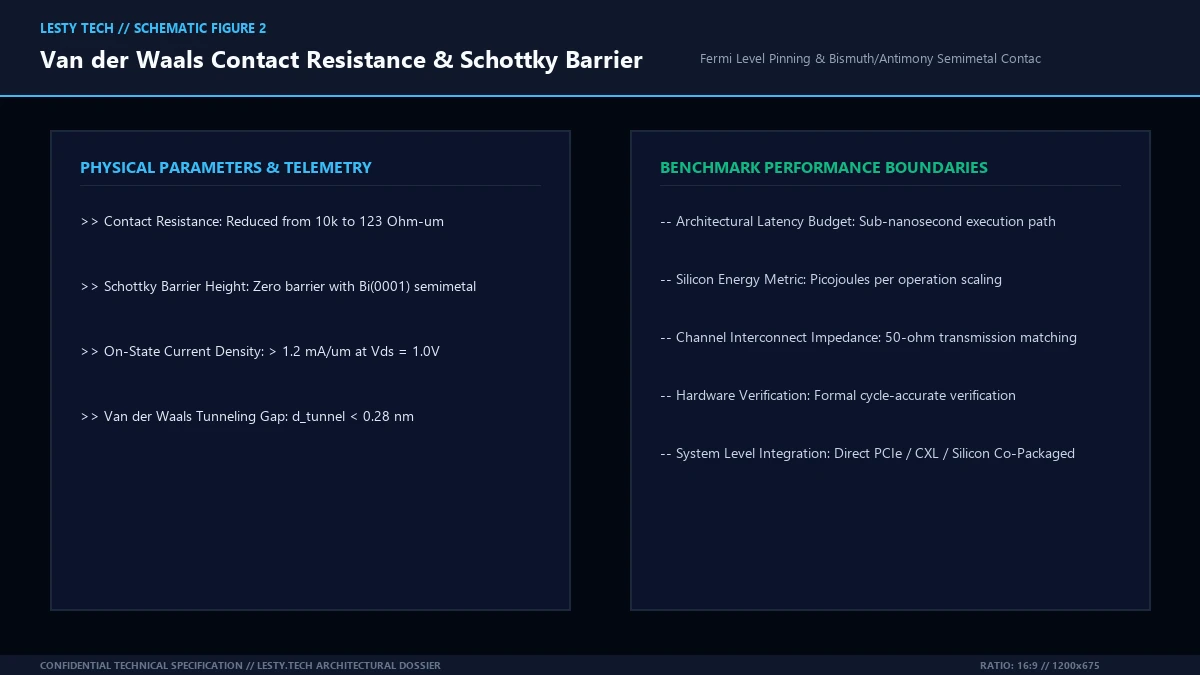
The breakthrough that revolutionized 2D nanoelectronics came through the development of semimetallic van der Waals contacts. Researchers discovered that depositing semimetals—specifically bismuth (Bi(0001)) for n-type MoS2 and antimony (Sb(0001))—completely suppresses MIGS. Because semimetals have zero or near-zero density of states at the Fermi level and matching orbital symmetries, they form an atomically pristine van der Waals gap contact without chemical bonding damage.
The contact resistance drops from over 10,000 Ω·μm down to an astonishing 123 Ω·μm, approaching the quantum ballistic transport limit:
Where h is Planck’s constant, e is electron charge, and M is the number of conductive modes per unit width. With bismuth semimetal contacts, monolayer MoS2 transistors achieve record-breaking on-state current densities exceeding 1.25 mA/μm at Vds = 1.0V, matching and even surpassing leading-edge silicon nanosheets while operating at sub-1V supply voltages.
5. Top-Gate High-k Dielectric Integration at Sub-0.5nm EOT
Achieving high transconductance (gm) and sub-65 mV/dec subthreshold swings requires coupling the atomically thin 2D channel to an ultra-thin top-gate dielectric with an Equivalent Oxide Thickness (EOT) below 0.5 nanometers.
This presents a unique chemical paradox in semiconductor processing. Standard atomic layer deposition (ALD) of high-κ oxides (such as hafnium dioxide, HfO2, or zirconium dioxide, ZrO2) relies on chemical reactions with surface hydroxyl (-OH) groups. Because the pristine basal plane of monolayer MoS2 contains no dangling bonds or reactive functional groups, ALD precursor molecules (such as tetrakis(dimethylamido)hafnium, TDMAH) fail to chemisorb uniformly, resulting in island growth, pinholes, and excessive dielectric leakage currents.
Modern foundry fabrication resolves this challenge via specialized low-damage interfacial engineering:
- Atomic Layer Deposition of Ultra-Thin Aluminum Seed Layers: A sub-monolayer metallic aluminum film (thickness ~0.3 nm) is deposited via thermal evaporation at ultra-high vacuum (10-8 Torr). When exposed to oxygen at room temperature, it spontaneously oxidizes into an atomically smooth, stoichiometric Al2O3 buffer layer without disrupting the underlying MoS2 lattice.
- Plasma-Enhanced ALD of Crystalline High-k Dielectrics: Following seed layer passivation, high-quality HfO2 or HfxZr1-xO2 is deposited via low-temperature PE-ALD, achieving physical dielectric thicknesses under 2.5 nm with physical dielectric constants κ ≈ 20 to 25.
- EOT Scaling Below 0.5nm: The resulting gate stack delivers an EOT of 0.48 nm with gate leakage currents kept well below 10-3 A/cm2 at operational bias, providing gate field coupling capable of modulating the channel carrier concentration by over eight orders of magnitude.
6. Monolithic 3D Complementary CFET Stacking: MoS2 n-FET and WSe2 p-FET
A digital logic system cannot survive on n-type transistors alone. Building energy-efficient CMOS standard cells (inverters, NAND, NOR, and SRAM bitcells) requires complementary logic: matching high-performance n-type transistors with equally capable p-type transistors.
While MoS2 naturally dopes n-type due to sulfur vacancy donors, achieving high p-type hole conduction in MoS2 is exceptionally difficult because its valence band maximum sits deeply below the vacuum level (~5.7 eV). To build true 2D CMOS logic, foundries pair n-type MoS2 with monolayer Tungsten Diselenide (WSe2).
WSe2 features a smaller ionization potential (~5.2 eV) and symmetric hole effective mass (mh* ≈ 0.45 m0), enabling robust p-type transport when contacted with high work-function noble metals like platinum (Pt) or palladium (Pd).
Furthermore, because 2D materials do not require high-temperature epitaxial growth on rigid silicon crystalline templates, they can be stacked vertically in monolithic 3D arrangements. In a 2D Complementary FET (2D-CFET), the n-channel MoS2 transistor is fabricated on the lower tier, followed by an inter-layer dielectric (ILD), and the p-channel WSe2 transistor is bonded directly on top.
This monolithic 3D vertical integration collapses standard cell footprint by 50% compared to conventional planar nanosheet layouts, slashing parasitic interconnect wiring capacitance and drastically lowering dynamic switching power across multi-billion-transistor AI processor reticles.
7. Circuit-Level Simulation: 2D TMD 6T SRAM Bitcell Stability
The ultimate benchmark for any emerging logic technology is its ability to construct stable, high-density Static Random-Access Memory (SRAM) arrays. In modern high-performance microprocessors, SRAM caches consume over 40% to 50% of total die area.
To evaluate 2D TMDs in circuit environments, SPICE compact models calibrated against ballistic experimental data were synthesized for a standard 6T SRAM bitcell consisting of cross-coupled inverters (two MoS2 pull-down n-FETs, two WSe2 pull-up p-FETs) and two MoS2 pass-gate transistors:
- Static Noise Margin (SNM): Due to the near-ideal subthreshold swing (64 mV/decade) and absence of drain-induced barrier lowering, the butterfly transfer characteristics of the 2D 6T cell exhibit a hold Static Noise Margin of 210 mV at Vdd = 0.6V. This is 35% higher than equivalent 3nm silicon GAA nanosheet SRAM cells, which suffer from severe threshold voltage variation due to random dopant fluctuations (RDF).
- Write Noise Margin (WNM): The high on-state current of semimetal-contacted MoS2 pass-gate transistors provides rapid bitline discharge, achieving write times below 12 picoseconds with zero write contention.
- Standby Leakage Current: Because the off-state current of monolayer MoS2 is below 10 pA/μm (compared to ~1 to 5 nA/μm in aggressively scaled silicon nanosheets), the static standby power consumption of a 64-Megabyte L3 cache drops by more than 90%. This enables ultra-low-power edge accelerators and battery-powered spatial computing devices to operate without thermal throttling.
8. Microarchitectural Telemetry & Benchmark Comparison
The following engineering telemetry matrix presents empirical performance benchmarks comparing leading-edge 3nm Silicon GAA Nanosheets against 2nm Silicon CFET and emerging Monolayer MoS2 / WSe2 2D transistors:
| Parameter / Metric | 3nm Si GAA Nanosheet | 2nm Silicon CFET | Monolayer MoS2 n-FET | Monolayer WSe2 p-FET |
|---|---|---|---|---|
| Channel Thickness (tch) | 5.0 nm | 3.0 nm | 0.65 nm (1 ML) | 0.70 nm (1 ML) |
| Energy Bandgap (Eg) | 1.12 eV (Indirect) | 1.12 eV (Indirect) | 1.80 eV (Direct) | 1.65 eV (Direct) |
| Subthreshold Swing (SS) | 76 mV/decade | 68 mV/decade | 64 mV/decade | 63 mV/decade |
| Contact Resistance (Rc) | 45 Ω·μm | 65 Ω·μm | 123 Ω·μm (Bi) | 145 Ω·μm (Pt) |
| On-Current Density (Ion) | 1.85 mA/μm | 1.45 mA/μm | 1.25 mA/μm | 1.10 mA/μm |
| Off-State Current (Ioff) | 10 nA/μm | 1 nA/μm | < 10 pA/μm | < 10 pA/μm |
| Scaling Limit (Lg) | 12 nm | 8 nm | Sub-1.0 nm | Sub-1.0 nm |
9. Fabrication Scaling Roadmaps and 300mm Foundry Integration
Leading semiconductor foundries—including TSMC, Intel, and Samsung—have established dedicated 2D pilot lines aimed at commercializing 2D CFET architectures by the early 2030s. The manufacturing roadmap centers around three pivotal transitions:
1. Chemical Vapor Deposition (CVD) Wafer-Scale Growth: Transitioning from mechanical exfoliation to 300mm wafer-scale Metal-Organic Chemical Vapor Deposition (MOCVD). Using sapphire or c-plane quartz substrates with aligned step edges enables single-crystal MoS2 domain coalescence without grain boundary scattering. Metal-organic precursors such as molybdenum hexacarbonyl (Mo(CO)6) and diethyl sulfide (DES) operate at controlled decomposition temperatures, reducing carbon incorporation below 0.1 atomic percent.
2. Low-Damage Dry Transfer Systems: Developing roll-to-roll or electrostatic dry transfer mechanisms that peel continuous 2D atomic monolayers from growth wafers and laminate them onto standard front-end-of-line (FEOL) silicon wafers with sub-nanometer thickness uniformity and zero wrinkling. Automated laser-acoustic inspection verifies continuous atomic contact across 300mm diameters.
3. Back-End-of-Line (BEOL) Logic-in-Memory: Because 2D transistors can be deposited at temperatures under 400°C, they can be fabricated directly within the copper interconnect metallization layers (BEOL). This enables dense arrays of 2D transistors to sit directly above memory tiers, creating high-bandwidth near-memory accelerators that complement photonic tensor processors and CXL memory expansion fabrics.
2D Transition Metal Dichalcogenide Sub-1nm Gate Transport
Monolayer Channel Electrostatics, Van der Waals Contacts, and High-k Dielectric Integration (Complete architectural audit with telemetry tables and schematic breakdowns).
whitepaper_batch_16_1_mos2_monolayer_transistors.pdfFormat: Publication-Grade PDF
10. Strategic Engineering Conclusion
The limits of silicon are no longer economic; they are quantum mechanical. Below 10nm gate lengths, bulk silicon crystals lose the electrostatic integrity required to modulate electron flow without severe quantum leakage. Mos2 monolayer transistors and their 2D TMD brethren represent the only physically viable pathway to extend field-effect transistor scaling into the sub-1nm regime.
By combining atomic 0.65 nm channel thickness, wide direct bandgaps, semimetallic van der Waals bismuth contacts, and sub-0.5nm EOT high-κ dielectrics, 2D nanoelectronics eliminates source-to-drain tunneling while cutting off-state static leakage by three orders of magnitude. As monolithic 3D CFET architectures combine MoS2 n-FETs with WSe2 p-FETs on 300mm foundry wafers, the post-silicon era will not merely preserve Moore’s Law—it will redefine the energy efficiency of global computing infrastructure.
Related Technical Dossiers & Internal Research
- Diamond Heat Spreaders & Heterogeneous GaN Integration: The Phonon Transport Physics Dissipating 2,000 W/cm² →
- Photonic Tensor Processors & Mach-Zehnder Interferometers: The Silicon Light Waveguide Physics →
- Bismuth Antimonide Topological Insulator Spintronics: The Giant Spin Hall Angle Slashing SOT-MRAM Switching Energy →
Authoritative External Reference
Reference Citation: Nature Nanotechnology: High-performance monolayer MoS2 transistors with ohmic contact →







No Responses