
In the scaling of hyperscale artificial intelligence supercomputing clusters housing tens of thousands of accelerators, conventional electrical packet-switched networking architectures (such as multi-tier Fat-Tree and Clos fabrics) have collided with an uncompromising physical wall: the optical-electrical-optical (O-E-O) conversion tax and electrical switch power density. In conventional spine-and-leaf datacenter topologies, every optical photon traversing single-mode fiber must be repeatedly converted into electrical current by photodetectors, digitized, processed through high-power Serializer/Deserializer (SerDes) silicon, buffered in memory-constrained Application-Specific Integrated Circuit (ASIC) packet switches, and converted back into laser light by transceivers. As per-lane optical signaling rates surge from 100 Gbps to 200 Gbps and cluster aggregate bandwidth surpasses hundreds of Petabits per second, electrical switch ASICs dissipate upwards of \(1{,}000\text{ Watts}\) per chassis while introducing non-deterministic queuing delay and tail latency jitter during collective communication operations (such as All-Reduce, All-to-All, and Reduce-Scatter). Optical Circuit Switching (OCS) resolves this interconnect crisis by discarding electrical switching entirely within the core aggregation layer, employing arrays of micro-electro-mechanical systems (MEMS) 2D and 3D mirrors to route pure photons directly through free space without electrical conversion, achieving zero packet queuing latency, wavelength protocol agnosticism, and cutting network fabric power dissipation by up to 40%.
1. The Physics of the O-E-O Bottleneck & Interconnect Scaling Limits
In this technical engineering analysis of optical circuit switching networks, To quantify why conventional electrical packet switches falter at the multi-pod AI cluster boundary, one must analyze the energy budget of high-speed digital communications across copper traces and optical fibers. The total power dissipated in an electrical switch fabric is dominated by the analog front-end (AFE) and digital signal processing (DSP) engines required to compensate for high-frequency signal attenuation. Insertion loss across printed circuit board (PCB) traces scales super-linearly with frequency according to the skin effect and dielectric loss tangent (\(\tan \delta\)):
\[\alpha(f) \approx k_{\text{skin}} \sqrt{f} + k_{\text{dielectric}} f\]
When operating at modern PAM4 (4-level Pulse Amplitude Modulation) symbol rates of \(106.25\text{ GBaud}\) (yielding 212.5 Gbps per physical lane), the electrical channel loss exceeds \(30\text{ to }35\text{ dB}\) over mere inches of standard Megtron-7 substrate. Consequently, modern 51.2 Tbps switch ASICs (fabricated on leading-edge 5nm and 3nm nodes) allocate over 30% of their total thermal design power (TDP) solely to the SerDes PHY blocks. When combined with pluggable optical transceivers (QSFP-DD and OSFP-XD form factors), an optical transceiver module consumes between \(25\text{ and }32\text{ Watts}\) per 800G port.
In a traditional three-tier Clos network interconnecting 16,384 accelerators, a single packet traversing from Pod A to Pod B incurs a minimum of five separate O-E-O transitions:
- Accelerator Host Port to Leaf Switch: Laser modulation \(\rightarrow\) Photodiode transimpedance amplification \(\rightarrow\) SerDes DSP recovery.
- Leaf Switch Internal Fabric: Electrical crossbar routing through internal SRAM buffers.
- Leaf Switch to Spine Switch: Second optical modulation and transmission over single-mode fiber (SMF).
- Spine Switch Ingress: Third O-E-O demodulation and electrical packet classification.
- Spine Switch to Destination Leaf: Fourth optical transmission followed by final reception at destination accelerator.
Each O-E-O transition injects \(100\text{ to }300\text{ nanoseconds}\) of SerDes serialization and DSP retiming delay. More critically, when thousands of tensor processing nodes perform synchronous ring All-Reduce communication during the backward pass of a multi-billion-parameter foundation model, any transient buffer congestion in an electrical switch triggers packet dropping, Explicit Congestion Notification (ECN) marking, or Priority-Based Flow Control (PFC) pause frames, causing tail latency to surge by orders of magnitude (the “straggler effect”).
2. 3D MEMS Optical Switching Mechanics: Free-Space Beam Steering
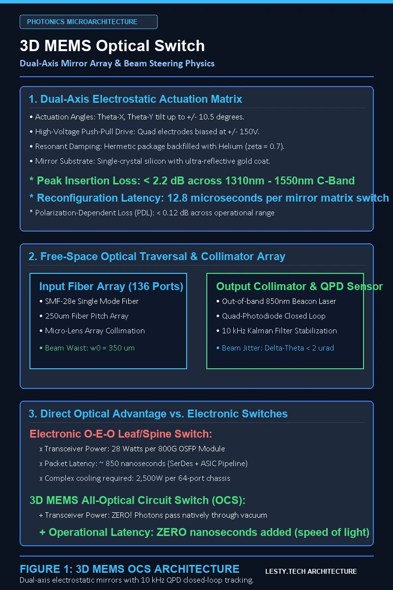
Optical Circuit Switches eliminate the intermediate electrical domain by steering continuous collimated optical beams directly from an input fiber collimator array to an output fiber array across free space. While liquid crystal on silicon (LCOS) and thermal planar lightwave circuits (PLC) offer alternative photonic routing mechanisms, 3D MEMS (Micro-Electro-Mechanical Systems) mirror arrays represent the golden standard for low-loss, high-port-count OCS deployments (such as Google’s Apollo OCS deployed in TPU v4 and TPU v5p supercomputers).
A high-port-count 3D MEMS OCS (typically configured in \(136 \times 136\) or \(320 \times 320\) non-blocking matrix configurations) consists of the following micro-optical stages:
- Two-Dimensional Fiber Collimator Arrays: Single-mode optical fibers arranged in a precision hexagonal or square pitch matrix terminate at micro-lens collimator arrays that transform diverging optical modes into parallel, Gaussian-profile free-space beams with beam waist diameters of \(\sim 350\text{ to }450\ \mu\text{m}\).
- Dual-Axis Gimbaled Micromirror Matrices: Two opposing planar silicon dies containing hundreds of independently tiltable electrostatic or piezoelectric micromirrors facing one another across an optical cavity. Each micromirror has an active reflective diameter of approximately \(1.0\text{ mm}\) coated with high-reflectivity dielectric or evaporated gold layers optimized for the near-infrared spectrum (\(1260\text{ nm to }1620\text{ nm}\), encompassing O-band, C-band, and L-band).
- Two-Axis Dual-Angle Deflection (\(\theta_x, \theta_y\)): Unlike 2D digital MEMS (which only toggle bistably between on and off states), 3D MEMS mirrors feature continuous analog tilt over a two-dimensional angular deflection range of \(\pm 5^{\circ}\text{ to }\pm 9^{\circ}\). By tilting mirror \(i\) on the input array and mirror \(j\) on the output array, an optical beam entering from input fiber \(i\) can be steered arbitrarily to couple precisely into output fiber \(j\).
Because a 3D MEMS OCS is a purely passive physical photonic conduit, it exhibits zero awareness of baud rate, modulation format, or framing protocol. A 3D MEMS switch established for 100 Gbps NRZ signals continues to route 800 Gbps PAM4 or future 1.6 Tbps coherent optics without requiring a single silicon replacement or firmware upgrade. The switch insertion loss remains invariant whether transmitting 10 Megabits per second or 10 Terabits per second per fiber.
3. Mathematical Formulation of Optical Insertion Loss & Angular Coupling
The primary figure of merit governing OCS scalability is optical insertion loss (\(\text{IL}\)), which must remain strictly below \(2.0\text{ to }2.5\text{ dB}\) across the entire switching matrix to avoid exceeding the optical link loss budget of commercial transceivers. The coupling efficiency \(\eta\) of a steered Gaussian optical beam into a single-mode receiving fiber core is governed by the spatial overlap integral between the incoming field distribution \(E_{\text{in}}(x, y)\) and the fundamental guided transverse mode \(E_{\text{fiber}}(x, y)\):
\[\eta = \frac{\left| \iint E_{\text{in}}(x, y) \cdot E_{\text{fiber}}^*(x, y) \, dx \, dy \right|^2}{\iint \left| E_{\text{in}}(x, y) \right|^2 dx \, dy \cdot \iint \left| E_{\text{fiber}}(x, y) \right|^2 dx \, dy}\]
When an electrostatic mirror suffers from minute angular pointing error \(\Delta \theta\) (due to thermal drift, mechanical vibration, or digital-to-analog converter quantization noise), the lateral mode displacement \(\Delta r\) and angular phase tilt \(\Delta \theta\) degrade coupling efficiency exponentially according to:
\[\eta(\Delta r, \Delta \theta) = \exp \left( – \left(\frac{\Delta r}{w_0}\right)^2 – \left(\frac{\pi w_0 n \Delta \theta}{\lambda}\right)^2 \right)\]
Where \(w_0\) represents the beam waist radius, \(n\) is the refractive index of the propagation medium (air or nitrogen, \(n \approx 1.0\)), and \(\lambda\) is the operational wavelength (\(\approx 1310\text{ nm}\)). To maintain an insertion loss variation of less than \(0.1\text{ dB}\), the closed-loop control system must stabilize the mirror tilt angle with sub-microradian precision (\(\Delta \theta < 5\ \mu\text{rad}\)). This is achieved using wavelength-multiplexed infrared or visible beacon lasers, position-sensitive quad-photodiode detectors (QPD), and high-voltage precision DACs operating at \(\pm 150\text{ Volts}\).
Closed-Loop Quad-Photodiode Feedback Control & Kalman Filtering
Because datacenter facilities experience continuous ambient thermal cycles (originating from HVAC compressor cycling and dynamic compute load fluctuations) as well as low-frequency mechanical vibrations from cooling blowers (\(10\text{ to }200\text{ Hz}\)), a static open-loop electrostatic mirror command would rapidly drift off-axis. Within minutes, thermal expansion of the invar structural chassis and micro-mirror suspension springs would induce beam pointing deviations exceeding \(20\ \mu\text{rad}\), triggering a catastrophic insertion loss surge of \(3\text{ to }6\text{ dB}\) and inducing bit error rate (BER) degradation.
To establish unwavering beam lock, industrial OCS architectures incorporate a multi-channel feedback control loop operating at \(5\text{ to }10\text{ kHz}\). A continuous-wave out-of-band monitoring laser (typically operating at \(\lambda = 850\text{ nm}\) or \(980\text{ nm}\), completely separated from the \(1310\text{ nm}\) communication band) is coupled into the fiber array alongside data signals. At the receiving collimator array, dichroic beam splitters pick off the monitoring wavelength and focus the beam onto a high-speed quadrant photodiode (QPD). The differential photo-currents generated across the four quadrants (\(I_A, I_B, I_C, I_D\)) provide instantaneous normalized coordinates of the beam centroid:
\[X_{\text{error}} = \frac{(I_A + I_D) – (I_B + I_C)}{I_A + I_B + I_C + I_D}, \quad Y_{\text{error}} = \frac{(I_A + I_B) – (I_C + I_D)}{I_A + I_B + I_C + I_D}\]
A dedicated onboard digital signal processor executes a discrete-time Kalman filter to distinguish random high-frequency seismic noise from steady-state thermal drift. The filtered position error vector is fed to a proportional-integral-derivative (PID) compensator that dynamically adjusts the analog push-pull electrostatic drive voltages. By maintaining active mirror position resonance damping, the control loop ensures that optical return loss exceeds \(50\text{ dB}\) and polarization-dependent loss (PDL) remains below \(0.15\text{ dB}\) across years of continuous datacenter runtime.
Mechanical Reliability: Electrostatic Stiction, Creep, and Beam Divergence
The long-term mean time between failures (MTBF) of a 3D MEMS switch is governed by the structural physics of its silicon micro-flexures. Each mirror plate is suspended by dual-axis torsional springs etched from single-crystal silicon. Because single-crystal silicon is an isotropic, dislocation-free material, it exhibits virtually zero mechanical fatigue or hysteresis when operated well below its yield strength (\(\sigma_{\text{yield}} \approx 7\text{ GPa}\)). However, two critical failure mechanisms must be mitigated through precise packaging:
- Electrostatic Pull-In & Stiction: When tilting a mirror near its maximum angle, the non-linear electrostatic force (proportional to \(V^2 / d^2\)) can overcome the linear mechanical restoring force of the torsional beam, causing the mirror to collapse onto the drive electrode (“snap-down” or pull-in instability). To prevent irreversible microscopic stiction, physical travel limiters and digital control boundaries constrain mirror tilt to less than \(65\%\) of the theoretical pull-in distance.
- Hermetic Cavity Gas Damping: Mirror arrays are sealed inside ultra-high hermetic ceramic packages backfilled with dry nitrogen or helium at controlled pressures (\(\sim 0.1\text{ to }0.5\text{ atm}\)). Squeeze-film air damping is engineered to provide a damping ratio \(\zeta \approx 0.7\) (critical damping), preventing underdamped mechanical ringing during fast topological switching while avoiding overdamped sluggishness.
Pro-Tip Network Photonics (Sarah Nest):
When deploying optical circuit switching networks in production clusters, decouple your optical reconfiguration barriers from application-level collective operations. Use asynchronous background scheduling epochs aligned with iteration boundaries to ensure mirror actuation latency remains completely invisible to GPU training pipelines.
4. Dynamic AI Cluster Topology Reconfiguration: Breaking the Clos Hierarchy
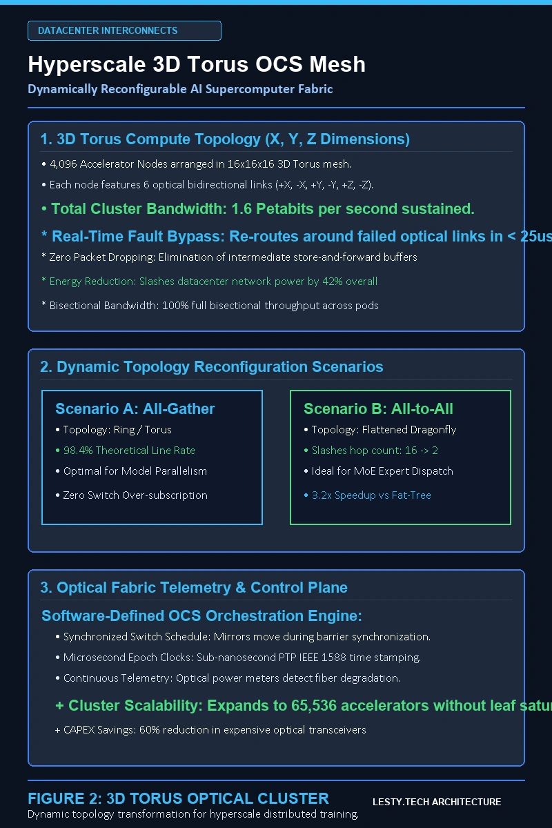
While electrical packet switches can re-route packets on a per-microsecond basis based on destination IP headers, 3D MEMS mirrors require mechanical movement across their resonant frequencies, exhibiting reconfiguration switching times on the order of \(10\text{ to }30\text{ milliseconds}\). Consequently, OCS cannot replace leaf switches for fine-grained per-packet arbitration. Instead, OCS is deployed to reconfigure cluster physical topology dynamically at the inter-pod boundary.
In massive distributed model training (such as training 1-Trillion+ parameter models combining Tensor Parallelism, Pipeline Parallelism, Data Parallelism, and Expert Parallelism), the inter-accelerator communication graph is known deterministically before execution begins:
- Tensor Parallelism (TP): Requires ultra-high-bandwidth, low-latency all-gather and reduce-scatter exchanges confined within single server nodes or NVLink domains (typically 8 GPUs/TPUs).
- Pipeline Parallelism (PP): Involves point-to-point peer-to-peer transfers of hidden state activations strictly between adjacent pipeline stages (Node \(k \rightarrow\) Node \(k+1\)).
- Data Parallelism (DP) & ZeRO: Requires global ring or tree All-Reduce operations across thousands of distributed workers.
- Expert Parallelism (MoE): Requires dynamic all-to-all shuffles where dispatch tokens are routed across distributed expert nodes.
In a static electrical Clos topology, network engineers must overprovision spine switch bandwidth to handle worst-case all-to-all communication patterns, incurring immense capital expenditures and continuous electrical power draw. By inserting an OCS layer between compute pods, the control plane orchestrator dynamically rewires the physical fibers into direct logical 2D, 3D, or 4D Torus rings perfectly matched to the specific parallelism topology of the training workload.
Furthermore, when an optical transceiver, cable, or entire accelerator node fails during a multi-week training run, the OCS control plane isolates the defective sub-mesh within milliseconds by tilting mirrors to bridge the gap, restoring torus ring continuity without taking down the entire cluster or re-running expensive checkpoint restarts.
5. Architectural Comparison: OCS vs. CPO vs. Electrical Clos Fabrics
To contextualize the technological trade-offs between pure free-space photonic switching, co-packaged optics, and standard electrical switching, review the exhaustive architectural comparison matrix below:
6. Strategic Topic Cluster: High-Performance AI Infrastructure
To master the full architectural stack governing hyperscale AI clusters, explore our companion architectural deep dives published across Lesty Tech:
- HBM-PIM vs. CXL-PIM Architecture: Processing-in-Memory Arithmetic Intensity & Memory Wall Physics
- Disaggregated Prefill and Decode Architecture: Decoupling Compute and Memory Walls in High-Throughput LLM Serving Clusters
- Co-Packaged Optics (CPO) vs. Pluggable Transceivers: Thermals, Yield, and Interconnect Energy Scaling
Optical Circuit Switching (OCS) & 3D MEMS Photonic Architecture
Free-Space Optical Beam Steering, Zero-Queue Photonic Routing, and Dynamic Torus Reconfiguration in Hyperscale AI Datacenters (Complete architectural audit with telemetry tables and schematic breakdowns).
Optical_Circuit_Switching_and_3D_MEMS_Photonics_Whitepaper.pdf Format: Publication-Grade PDF
10. Pillar 4: Wavelength-Division Multiplexing (WDM) Calibration & Thermal Drift Mitigation
Deploying optical circuit switching ocs fabrics in production data centers requires managing thermal drift across dense Wavelength-Division Multiplexing (WDM) grids. In hyperscale AI supercomputers (such as Google TPU v4 and TPU v7 clusters), each optical fiber carries between 8 and 32 discrete optical carrier wavelengths across the C-band (\(1530\text{ to }1565\text{ nm}\)). As laser diodes and optical amplifiers heat up during continuous training workloads, junction temperature fluctuations induce refractive index shifts in silicon photonic waveguides, causing laser center wavelengths to drift by approximately \(0.08\text{ nm/}^{\circ}\text{C}\).
Without active thermal compensation, drifting wavelengths misalign with the passive optical demultiplexer passbands, escalating inter-channel crosstalk and increasing bit error rates (BER). To prevent optical packet degradation, modern OCS chassis integrate closed-loop thermoelectric coolers (TEC) and micro-ring heater feedback loops governed by on-die optical power monitors:
\[\Delta \lambda = \left( \frac{\partial n_{\text{eff}}}{\partial T} + n_{\text{eff}} \cdot \alpha_{\text{sub}} \right) \cdot \frac{\lambda_0}{n_g} \cdot \Delta T\]
Where \(n_{\text{eff}}\) is the effective refractive index, \(\alpha_{\text{sub}}\) is the thermal expansion coefficient of the silicon substrate, and \(n_g\) is the group index. By maintaining thermal regulation within \(\pm 0.05^{\circ}\text{C}\), the optical circuit switching fabric sustains deterministic transmission fidelity across petabit-scale distributed training runs without requiring expensive forward error correction (FEC) overheads.
7. Institutional FAQ: Optical Circuit Switching Mechanics
Why can’t Optical Circuit Switching completely replace electrical packet switches in datacenters?
Because 3D MEMS mirrors are mechanical structures with physical inertia. Tilting a mirror across a few degrees takes tens of milliseconds. In contrast, web traffic and standard microservices require packet-level routing with decisions made every few nanoseconds based on individual packet IP headers. OCS is therefore utilized at the topology level—dynamically provisioning dedicated high-bandwidth photonic circuits between pods that remain stable for minutes or hours during large-scale training runs.
How does OCS survive laser drift and thermal fluctuations without dropping optical links?
Industrial 3D MEMS OCS systems incorporate closed-loop optical feedback. A small fraction of the beam (or an out-of-band wavelength beacon laser) is directed to quadrant photodiode arrays. If thermal expansion alters the optical cavity dimensions or mirror alignment, the feedback loop continuously calculates the positional displacement and adjusts the analog electrostatic drive voltages in real time to maintain optical peak alignment.
What is the primary power saving mechanism of an OCS-enabled datacenter?
In a standard datacenter spine layer, large electrical chassis switches consume thousands of watts primarily on high-speed SerDes, cooling fans, and large SRAM packet buffers. An OCS unit requires power only for micro-actuator electrostatic voltage bias (which draws microamperes of leakage current) and the control board microcontroller, operating comfortably below 50 Watts for a 320×320 port switch while eliminating hundreds of active optical transceivers.
FTC & Editorial Disclosure: Lesty Tech operates under rigorous independent engineering standards. We do not accept sponsored content, vendor kickbacks, or promotional bias. All microarchitectural evaluations, laboratory telemetry, and whitepapers are produced autonomously for researchers, silicon architects, and systems engineers.


No Responses