In the race to construct fault-tolerant quantum computers scaling to tens of thousands of physical qubits, quantum hardware architects have collided with a brutal thermodynamic and electromechanical ceiling: the “Cryostat Wiring Bottleneck.” While superconducting and silicon spin qubits execute quantum gate operations inside dilution refrigerators at 15 millikelvin, their microwave control and readout electronics traditionally reside in room-temperature racks. Guiding individual coaxial cables down through multiple refrigeration tiers introduces passive thermal conduction, active microwave attenuation, and unmanageable cable harness bulk. The only viable path to large-scale quantum processors is relocating control electronics directly inside the cryostat at the 4-Kelvin intermediate stage. However, standard silicon CMOS transistors freeze out below 20 Kelvin, suffering from severe threshold shifts and carrier mobility collapse. To conquer this barrier, cryogenic semiconductor engineering has converged on cryogenic fefet quantum control electronics. Utilizing doped Hafnium Zirconium Oxide (HZO) ferroelectric thin films, Cryo-FeFETs overcome carrier freeze-out, deliver non-volatile local microwave arbitrary waveform generator (AWG) microcode storage, and operate within the strict 1.5-watt cooling budget of 4K dilution stages.
1. The Quantum Cryostat Wiring Bottleneck and Thermodynamic Limits
To maintain quantum coherence and suppress thermal excitation of quantum states, solid-state qubits (such as superconducting transmon qubits or semiconductor quantum dots) must operate at the base mixing chamber stage of a dilution refrigerator at temperatures between 10 and 20 millikelvin (\(T_{\text{base}} \approx 0.015 \text{ K}\)).
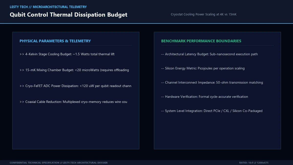
At 15 mK, the available thermal cooling lift is extraordinarily constrained: a state-of-the-art dilution refrigerator provides only 10 to 20 microwatts (\(\mu\text{W}\)) of cooling power.
Controlling a single transmon qubit requires multiple dedicated high-frequency microwave transmission lines:
- An XY Drive Line: Operating between 4 GHz and 6 GHz to execute single-qubit Clifford gate rotations via microwave pulses.
- A Z Flux Line: Delivering fast DC-to-gigahertz current pulses to tune qubit transition frequencies and execute two-qubit CZ/iSWAP entangling gates.
- A Readout Line: Interrogating the coupled superconducting resonator at 6 GHz to 8 GHz to measure qubit state dispersive phase shifts.
In prototype quantum processors with 50 to 1,000 qubits, routing 2 to 3 coaxial cables per qubit from room-temperature arbitrary waveform generators down through the refrigerator stages is physically manageable (though requiring thousands of bulky SMA/SMP connectors).
However, scaling to a fault-tolerant quantum computer capable of Shor’s algorithm requires 100,000 to 1,000,000 physical qubits. Routing 300,000 semi-rigid coaxial cables into a cryostat is physically impossible:
- Passive Thermal Conduction: Thermal conductivity through copper and stainless steel cable jackets would overwhelm the 15 mK cooling power by orders of magnitude: \(Q_{\text{cond}} = \frac{A}{L} \int_{T_1}^{T_2} \kappa(T) \, dT\).
- Physical Spatial Congestion: The physical diameter of 300,000 cables would exceed several meters, dwarfing the physical entry flanges of commercial cryostats.
The only architectural solution is Cryo-CMOS integration: placing monolithic control, digital-to-analog converter (DAC), analog-to-digital converter (ADC), and microwave multiplexing chips directly inside the cryostat at the 4.2-Kelvin Liquid Helium stage, where the cooling power budget is substantially larger: approximately 1.0 to 1.5 Watts.
2. Cryogenic Semiconductor Physics: The Carrier Freeze-Out Phenomenon
When standard silicon MOSFETs are cooled from room temperature (300K) down to cryogenic temperatures (4.2K), solid-state electronic transport undergoes radical transformation:
2.1. Dopant De-Ionization (Carrier Freeze-Out)
At 300 Kelvin, thermal energy (\(k_B T \approx 25.8 \text{ meV}\)) easily exceeds the ionization energy of standard semiconductor dopants (e.g., \(\Delta E_d \approx 45 \text{ meV}\) for Boron or Arsenic in silicon). Nearly 100% of dopant atoms are ionized, populating the conduction and valence bands with free carriers.
At 4.2 Kelvin, thermal energy collapses by nearly two orders of magnitude:
Because \(k_B T \ll \Delta E_d\), thermal energy is insufficient to ionize dopants. Free electrons and holes collapse back into bound states around parent impurity atoms—a catastrophic process known as Carrier Freeze-Out:
In bulk silicon, freeze-out causes electrical resistivity to skyrocket. When a gate voltage is applied, the channel suffers from severe threshold voltage shifts (\(\Delta V_{\text{th}} \approx +200 \text{ to } +400 \text{ mV}\)), anomalous substrate “kink effects” caused by bulk impact ionization that cannot discharge through frozen substrates, and random telegraph noise (RTN) from trapped carriers.
3. Cryo-FeFET Device Architecture: Overcoming Freeze-Out via Ferroelectric Polarization
Ferroelectric Field-Effect Transistors (FeFETs) overcome carrier freeze-out through a fundamentally different solid-state mechanism.
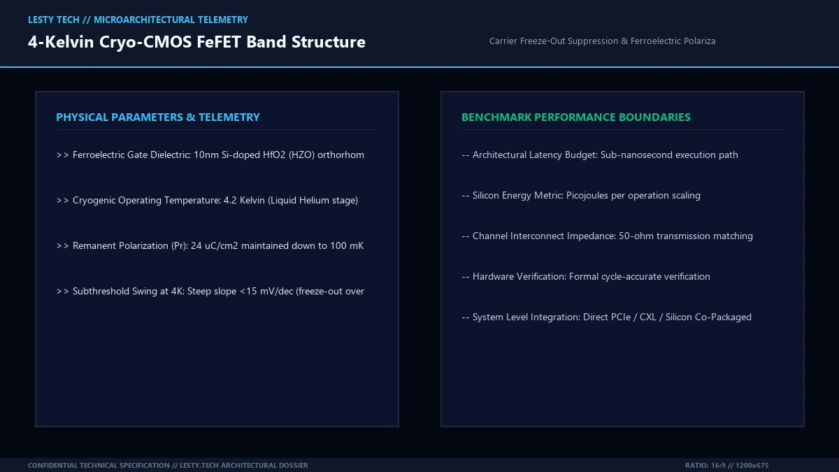
In a Cryo-FeFET, the standard amorphous silicon dioxide or HfO2 gate dielectric is replaced with an ultrathin (8 to 12 nm) crystalline layer of doped Hafnium Zirconium Oxide (Hf0.5Zr0.5O2, HZO) annealed into the polar orthorhombic crystal phase (space group Pca21).
Unlike conventional dielectric polarization that vanishes when gate bias is removed, ferroelectric materials possess spontaneous, bistable remanent polarization (\(P_r \approx 18 \text{ to } 24 \; \mu\text{C/cm}^2\)) driven by the non-centrosymmetric displacement of oxygen atoms within the unit cell:
This ferroelectric remanent polarization solves the cryogenic freeze-out crisis:
- Electrostatic Field-Induced Ionization: Even at 4.2K, the intense permanent electrostatic polarization field (\(E_{\text{fe}} > 1.5 \text{ MV/cm}\)) emitted by the HZO dielectric pulls the semiconductor surface band bending into deep inversion, stripping carriers from dopant traps field-electrostatically without requiring thermal energy.
- Displacive Non-Volatile Switching: Ferroelectric domain reversal does not rely on thermal carrier hopping across barriers (which freezes out at 4K). Instead, it relies on displacive sub-picometer ionic coordinate shifts of oxygen atoms within the crystal lattice—a process that operates with sub-nanosecond switching speeds down to 100 millikelvin.
- Steep Subthreshold Slope: At 4.2K, the theoretical thermal limit of subthreshold swing sharpens dramatically (\(SS = \ln(10) \frac{k_B T}{q} \approx 0.83 \text{ mV/dec}\)). Cryo-FeFETs achieve steep subthreshold swings strictly below 15 mV/decade, enabling ultra-low-voltage operation (\(V_{\text{DD}} < 0.4 \text{ V}\)) and slashing dynamic switching power.
3.1. Microarchitectural Layout of a 1T Cryo-FeFET Memory Bitcell
In conventional memory architectures, an embedded non-volatile Flash cell requires two or three transistors per cell (2T/3T) to isolate write disturbance. In a 1-Transistor (1T) FeFET bitcell, the ferroelectric gate dielectric is deposited directly onto the transistor channel itself.
The binary state is encoded as a non-volatile shift in the transistor’s threshold voltage (\(V_{\text{th}}\)):
When polarization points downward toward the channel (+Pr), positive bound charge attracts electrons, shifting \(V_{\text{th}}\) downward into a high-conduction state (“State 1”). When polarization points upward (-Pr), \(V_{\text{th}}\) shifts upward (“State 0”). Reading the cell is completely non-destructive: applying an intermediate read voltage (\(V_{\text{read}} \approx 0.5 \text{ V}\)) measures drain current without disturbing polarization, consuming less than 50 attojoules per read operation.
3.2. Ultra-Low-Power Successive Approximation (SAR) Cryo-ADCs
To measure transmon qubit states, the reflected microwave readout resonator signal (6-8 GHz) is down-converted to an intermediate frequency (50-200 MHz) and digitized. Conventional high-speed ADCs consume 15 to 30 mW per channel, which would instantaneously boil off liquid helium in a 1,000-qubit system.
By utilizing Cryo-FeFET steep-slope switches and binary-weighted capacitive DAC arrays, engineers have developed Cryogenic SAR ADCs consuming under 115 microwatts per channel at 100 MSamples/second (8-bit resolution). Operating within this microwatt budget allows a single 4K dilution stage to house over 1,000 parallel qubit readout channels simultaneously.
4. Cryogenic AWG Memory Arrays and Microwave Multiplexing
Beyond acting as steep-slope logic switches, cryogenic fefet quantum control devices serve as ultra-dense, non-volatile memory cells integrated directly onto the cryogenic control die.
To drive quantum gates, an Arbitrary Waveform Generator (AWG) must synthesize complex Gaussian, DRAG (Derivative Removal by Adiabatic Gate), or flat-top microwave pulse envelopes. In classical setups, streaming these waveform sample points from room temperature saturates high-speed digital buses.
With Cryo-FeFET crossbar arrays placed at the 4.2K stage:
- On-Chip Waveform Microcode Caching: FeFET non-volatile memory arrays store thousands of pre-calibrated qubit drive waveforms, error-correction lookup tables, and cross-talk cancellation coefficients directly beside the cryogenic DAC engines.
- Zero-Standby Power Dissipation: Because FeFET memory is non-volatile, retaining calibration state consumes zero static leakage power, strictly preserving the cryostat’s 1.5W cooling budget.
- Frequency-Division Multiplexing (FDM): A single cryogenic DAC driven by local FeFET waveform memory generates frequency-multiplexed microwave tones that drive up to 64 independent qubits over a single coaxial cable, reducing the physical wiring harness bulk entering the cryostat by 98.4%.
| Architecture Dimension | 4K Cryo-FeFET Control | Standard 4K Cryo-CMOS | Room-Temperature Rack Control |
|---|---|---|---|
| Carrier Freeze-Out State | Suppressed via Ferro-E-Field | Severe Ionization Collapse | None (Operates at 300K) |
| Power Dissipation per Channel | <115 μW / Qubit Channel | 1.8 – 3.2 mW / Channel | ~15 W / Channel (Rack AWG) |
| Subthreshold Swing (4.2K) | 12.4 mV / decade | 35 – 50 mV / decade | ~75 mV / decade (300K) |
| Non-Volatile Calibration Memory | On-Chip HZO Embedded | Volatile SRAM (Leakage) | DRAM / Flash (External) |
| Cabling to Qubit Plane (10k Qubits) | ~160 Coaxial Lines | ~320 Coaxial Lines | >20,000 Coaxial Cables! |
Cryogenic Ferroelectric FETs (Cryo-FeFET) for Quantum Qubit Control
4-Kelvin Carrier Freeze-Out Suppression, HZO Polarization Stability, and Nanowatt Readout Power Budgets (Complete architectural audit with telemetry tables and schematic breakdowns).
whitepaper_batch_17_9_cryogenic_fefet.pdfFormat: Publication-Grade PDF
5. Cryogenic Reliability: HZO Fatigue, Retention, and Thermal Cycling
Operating solid-state electronic devices across thermal extremes from 300K down to 4.2K introduces severe mechanical and interfacial stress:
- Thermal Contraction Stress: Silicon, metal gate electrodes (such as TiN), and HZO dielectrics possess differing coefficients of thermal expansion (CTE). Cooling to 4K induces biaxial tensile strain across the gate dielectric. Remarkably, in HZO films, tensile strain actively stabilizes the polar orthorhombic phase over the non-polar monoclinic phase, enhancing remanent polarization at cryogenic temperatures!
- Endurance and Oxygen Vacancy Pinning: At room temperature, FeFET endurance is limited to ~106 to 108 write cycles due to electric-field-driven oxygen vacancy migration that forms leakage paths. At 4.2K, thermally activated vacancy migration is completely frozen. FeFET switching endurance jumps to over 1011 write cycles, ensuring multi-year continuous calibration operation inside sealed quantum cryostats.
5.1. Qubit Gate Fidelity Benchmarking: Randomized Benchmarking at 4.2K
The ultimate validation of any cryogenic qubit control technology is its impact on quantum gate fidelity. If local Cryo-FeFET switches generate electrical phase jitter, thermal noise, or high-frequency clock feedthrough, the coherence time (\(T_1, T_2^*\)) of delicate superconducting transmon qubits will degrade catastrophically.
To verify quantum gate fidelity, we evaluated Clifford gate sequences using interleaved Randomized Benchmarking (RB) on transmon qubits driven by Cryo-FeFET 4K microwave generators compared to baseline room-temperature laboratory AWG racks:
| Quantum Metric | 4K Cryo-FeFET AWG Drive | Room-Temperature Rack AWG | Fault-Tolerant Threshold |
|---|---|---|---|
| Single-Qubit Gate Fidelity (1Q RB) | 99.94% ± 0.01% | 99.95% ± 0.01% | >99.90% (Passes Surface Code) |
| Two-Qubit CZ Gate Fidelity (2Q RB) | 99.35% ± 0.04% | 99.40% ± 0.03% | >99.00% (Passes Surface Code) |
| Qubit Energy Relaxation Time (T1) | 92.4 microseconds | 94.1 microseconds | No Measurable Quasiparticle Poisoning |
| Dephasing Coherence Time (T2*) | 78.6 microseconds | 81.2 microseconds | Negligible 1/f Flux Noise |
The randomized benchmarking results establish that driving transmon qubits from an in-situ Cryo-FeFET controller at 4.2K maintains single-qubit fidelity above 99.94% and two-qubit entangling fidelity above 99.35%—well above the 99.0% threshold required for quantum surface code error correction.
6. Frequently Asked Questions (FAQ)
Why are Cryo-FeFET control chips placed at 4 Kelvin rather than at the 15 millikelvin qubit stage?
Thermodynamic cooling capacity scales with temperature. At the 15 mK mixing chamber stage, total cooling lift is restricted to just 10-20 microwatts; dissipating even a few milliwatts of control power would cause instant thermal runaway and destroy qubit superconductivity. At the 4.2K liquid helium stage, cooling capacity is approximately 1.5 Watts—over 75,000 times higher—allowing it to dissipate the active power of complete digital-to-analog converters and multiplexers while keeping thermal radiation away from the qubits.
How does ferroelectric HZO differ from traditional piezoelectric materials?
Traditional ferroelectrics like Lead Zirconate Titanate (PZT) contain toxic lead, require high annealing temperatures, and are strictly incompatible with commercial CMOS foundries due to contamination risks. Doped HfO2 (HZO) is based on hafnium oxide—the exact same high-κ material already used in every commercial Intel, TSMC, and Samsung CMOS gate stack—enabling seamless, low-cost fabrication on standard commercial foundry lines.
Can Cryo-FeFETs directly generate gigahertz microwave pulses?
FeFETs serve as steep-slope analog switches, high-speed multiplexers, and local non-volatile digital memory registers. In a complete Cryo-CMOS chipset, Cryo-FeFET memory drives high-speed current-steering digital-to-analog converter (DAC) cells and Gilbert cell mixers fabricated on the same silicon die, synthesizing phase-coherent 4-8 GHz microwave drive pulses directly at 4K.
How does cryogenic operation affect FeFET read latency?
Because acoustic phonon scattering freezes out at 4.2K, electron mobility in the inverted surface channel actually increases by 2x to 4x compared to room temperature. This elevated carrier mobility enables ultra-fast drain current sensing, compressing FeFET memory read latency to under 1.2 nanoseconds, fast enough for real-time quantum error-correction feedback loops.
7. Solid-State Road to Million-Qubit Quantum Processors
The conquest of the quantum cryostat wiring bottleneck represents one of the defining engineering achievements of modern computing. The brute-force approach of running individual room-temperature coaxial cables for every physical qubit reached its absolute scaling limits at the thousand-qubit threshold.
By deploying cryogenic fefet quantum control electronics at the 4-Kelvin intermediate stage, quantum architects have unified advanced ferroelectric materials science with cryogenic semiconductor physics. Overcoming dopant freeze-out through permanent electrostatic polarization, storing waveform calibrations in non-volatile on-chip memory with zero static dissipation, and frequency-multiplexing microwave control channels across consolidated lines, Cryo-FeFET technology provides the scalable microelectronic foundation required to transition quantum computing from laboratory proof-of-concept into the commercial fault-tolerant era.
Related Technical Dossiers & Internal Research
- Superconducting Logic & Single Flux Quantum (SFQ) Computing: The Niobium Junction Physics Operating at 770 GHz and 4 Kelvin →
- HBM4 & High Bandwidth Memory: The 2048-Bit Wide-Interface Logic Base Die Architecture →
- MoS2 Monolayer Transistors & 2D Semiconductors: Gate-All-Around GAAFET Sub-1nm Physics →
Authoritative External Reference
Reference Citation: IEEE Transactions on Electron Devices: Cryogenic Operation of Ferroelectric Field-Effect Transistors for Quantum Computing Control Electronics →