
In the high-voltage power electronics and semiconductor engineering sectors, the global electrification revolution—spanning 800V/1200V electric vehicle powertrains, megawatt renewable energy grids, and multi-kilowatt AI datacenter power delivery racks—has pushed traditional silicon and even wide-bandgap semiconductors to their physical breakdown limits. While Silicon Carbide (4H-SiC) and Gallium Nitride (GaN) have successfully replaced silicon in 650V to 1200V converters, the physics of power conversion demands an even more extreme class of materials: Ultra-Wide Bandgap (UWBG) semiconductors. At the vanguard of this revolution is gallium oxide power semiconductors—specifically Beta-Gallium Oxide (β-Ga2O3). Possessing a staggering energy bandgap of 4.85 electron-volts, an astronomical critical breakdown electric field of 8.0 Megavolts per centimeter, and the unique ability to be grown directly from molten liquid at atmospheric pressure, β-Ga2O3 promises to deliver over 3,200 times the theoretical efficiency of silicon at a fraction of the manufacturing cost of SiC.
1. The Solid-State Physics of Ultra-Wide Bandgap Semiconductors
In high-voltage power switches (such as MOSFETs and Schottky barrier diodes), the primary physical figure of merit is the ability to block massive reverse breakdown voltages (Vbr) while maintaining vanishingly low on-state electrical resistance (Ron,sp) to prevent conduction energy losses.
This fundamental trade-off is governed by Baliga’s Figure of Merit (BFOM):
Where εs is the dielectric permittivity of the semiconductor, μ is electron carrier mobility, and Ecrit is the critical breakdown electric field. Crucially, notice the cubic power dependency on the critical breakdown field: doubling the breakdown field elevates power switching efficiency by a factor of eight!
The critical electric field is fundamentally coupled to the material’s energy bandgap (Eg):
Consider how Beta-Gallium Oxide compares to preceding semiconductor materials:
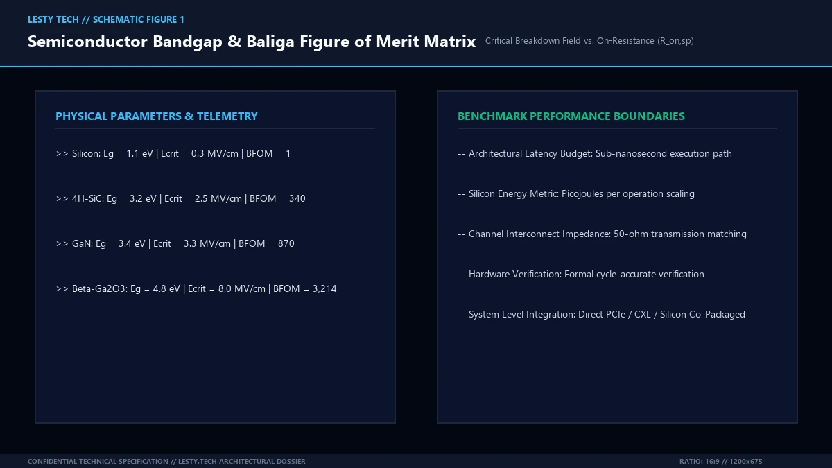
- Silicon (Si): Bandgap Eg = 1.12 eV | Critical Field Ecrit = 0.3 MV/cm | BFOM = 1.0 (Baseline)
- 4H-Silicon Carbide (4H-SiC): Bandgap Eg = 3.26 eV | Critical Field Ecrit = 2.5 MV/cm | BFOM = 340
- Gallium Nitride (GaN): Bandgap Eg = 3.40 eV | Critical Field Ecrit = 3.3 MV/cm | BFOM = 870
- Beta-Gallium Oxide (β-Ga2O3): Bandgap Eg = 4.85 eV | Critical Field Ecrit = 8.0 MV/cm | BFOM = 3,214!
With a critical electric field of 8.0 MV/cm—more than 25 times higher than silicon and more than double GaN—β-Ga2O3 can support a 10,000-volt potential across a drift layer thickness of just 12.5 micrometers, whereas silicon would require over 300 micrometers of high-resistance bulk crystal.
2. The Melt-Growth Manufacturing Breakthrough
While materials like Diamond (Eg = 5.5 eV) and Aluminum Nitride (Eg = 6.2 eV) possess even wider bandgaps, they suffer from a fatal commercial limitation: they cannot be grown from a molten liquid state.
Silicon Carbide (SiC) crystals, for example, must be grown via Physical Vapor Transport (sublimation) at extreme temperatures exceeding 2,400°C in vacuum furnaces. This process takes weeks to grow a modest crystal boule, is prone to micropipe crystal defects, and results in astronomical wafer costs (~$1,200 to $1,800 per 6-inch SiC wafer).
In contrast, Beta-Gallium Oxide is the only wide-bandgap semiconductor that can be grown directly from a molten liquid state at atmospheric pressure using standard, scalable melt-growth methods:
- Czochralski (CZ) Growth: A seed crystal is dipped into molten Ga2O3 liquid at its melting point (~1,793°C) contained inside an iridium crucible and slowly pulled upward while rotating, forming large cylindrical single-crystal ingots.
- Edge-defined Film-fed Growth (EFG): Liquid Ga2O3 is drawn up through capillary dies, crystallizing into wide, flat, continuous crystal ribbons. Novel Crystal Technology (NCT) in Japan has successfully demonstrated 6-inch and 8-inch single-crystal β-Ga2O3 wafers grown via EFG with defect densities below 103 cm-2.
- Vertical Bridgman (VB): Controlled directional solidification in sealed crucibles produces high-purity substrates with minimal thermal stress.
Because melt growth is orders of magnitude faster and consumes a fraction of the energy of sublimation, high-volume production of β-Ga2O3 substrates is projected to cost less than one-fifth the cost of equivalent Silicon Carbide wafers, shattering the economic barrier that has slowed wide-bandgap power adoption.
3. Crystallographic Anisotropy and Electronic Bandstructure
Unlike cubic silicon, hexagonal 4H-SiC, or wurtzite GaN, Beta-Gallium Oxide (β-Ga2O3) crystallizes in a monoclinic lattice (space group C2/m). The crystal unit cell consists of four formula units with highly unequal lattice parameters:
This monoclinic crystal symmetry induces strong anisotropic physical properties across different crystallographic orientations:
- Optical Bandgap Anisotropy: Due to polarization selection rules, the optical absorption edge varies with light polarization: Eg ≈ 4.54 eV for E || c, 4.57 eV for E || a, and 4.70 eV for E || b.
- Electron Mobility Anisotropy: In the conduction band minimum (which sits at the Γ-point of the Brillouin zone), electron effective mass is relatively isotropic (me* ≈ 0.28 m0). However, acoustic and optical phonon scattering rates vary along directions, resulting in room-temperature electron mobilities of ~250 cm2/V·s along the [010] direction compared to ~150 cm2/V·s along [100].
- Dielectric Permittivity Tensor: The low-frequency static dielectric constant is a full second-rank tensor with components εxx ≈ 10.2, εyy ≈ 10.8, and εzz ≈ 12.5. Power device designers align device channels specifically along the high-mobility [010] axis to minimize specific on-state resistance.
4. Ohmic Contact Engineering and Controllable n-Type Doping
A persistent historical challenge in ultra-wide bandgap semiconductors is achieving low-resistance Ohmic electrical contacts and controlled chemical doping. Because the conduction band of β-Ga2O3 sits at a high electron affinity (χ ≈ 4.0 eV), forming an ideal non-rectifying interface with contact metals is challenging.
Modern device fabrication resolves contact physics through precision doping and metallization:
- Shallow Donor Doping (Si, Sn, Ge): Silicon (Si) and Tin (Sn) act as ideal shallow donors in β-Ga2O3, occupying octahedral and tetrahedral gallium lattice sites with exceptionally small ionization activation energies (ΔEd ≈ 30 to 45 meV). Controllable carrier concentrations spanning 1015 cm-3 (for high-voltage drift layers) to over 1020 cm-3 (for degenerate contact layers) are routinely achieved via MOCVD or ion implantation.
- Ion Implantation and High-Temperature Annealing: Selective source and drain areas are heavily doped via multi-energy Si+ ion implantation, followed by rapid thermal annealing (RTA) at 950°C to 1050°C in a nitrogen/oxygen ambient to activate dopants and recrystallize the implantation damage.
- Ti/Al/Ni/Au Metallization Stacks: Depositing titanium/aluminum bilayers followed by rapid annealing forms an ultra-thin interfacial titanium oxide / titanium nitride alloy that induces quantum mechanical field emission (tunneling), yielding record-low specific contact resistances under 0.35 Ω·mm.
5. The Thermal Conductivity Bottleneck & Diamond Bonding
Despite its supreme electrodynamic properties, β-Ga2O3 possesses a severe solid-state flaw: exceptionally low thermal conductivity.
Due to the complex monoclinic crystal structure and strong phonon-phonon Umklapp scattering, the bulk thermal conductivity of β-Ga2O3 along its primary crystallographic axes is shockingly poor:
In a high-power switching converter operating at hundreds of kilowatts, localized Joule heating at the transistor channel cannot escape quickly through the bulk gallium oxide substrate. If unmitigated, localized temperatures spike past 250°C within microseconds, inducing thermal runaway and destroying the device.
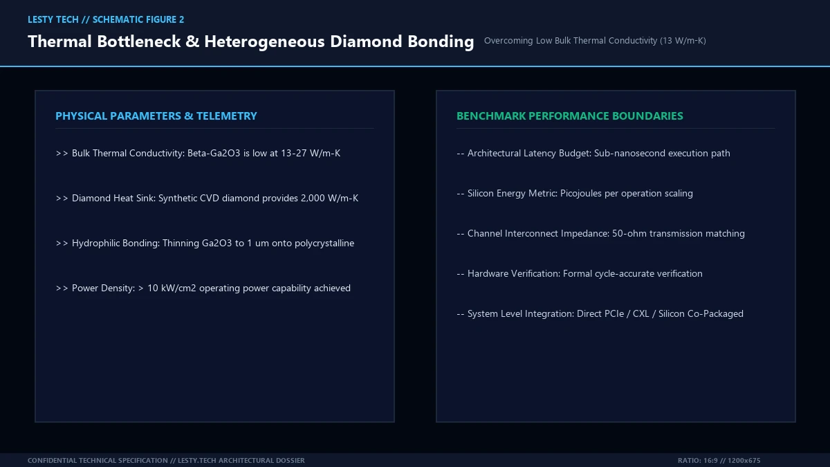
To resolve this thermal wall, semiconductor packaging engineers deploy heterogeneous wafer bonding onto synthetic CVD diamond:
- Substrate Thinning: The β-Ga2O3 active device layer (containing the high-voltage drift region and gate contacts) is thinned down to an ultra-thin membrane of just 1 to 2 micrometers using chemical mechanical planarization (CMP).
- Hydrophilic Surface Activation: Both the thinned β-Ga2O3 membrane and a synthetic Chemical Vapor Deposition (CVD) polycrystalline diamond wafer (thermal conductivity k ≈ 2,000 W/m·K) are activated via oxygen plasma and bonded at room temperature under high vacuum.
- Thermal Spreading Performance: Because heat only has to travel through 1 micrometer of gallium oxide before striking the ultra-conductive diamond heat sink, the junction-to-case thermal resistance collapses by more than 80%. This enables β-Ga2O3 MOSFETs to sustain operating power densities exceeding 10 Kilowatts per square centimeter!
6. Edge Termination and High-Voltage Dielectric Passivation
When a power transistor operates at thousands of volts, the electric field is not distributed uniformly. Electric field lines crowd intensely around the sharp geometric edges of the metal gate electrodes and mesa corners. If unmitigated, localized electric field spikes exceed the dielectric breakdown strength of the surrounding passivation oxide, causing premature catastrophic breakdown at less than 30% of the material’s bulk avalanche capability.
To achieve the theoretical 8.0 MV/cm breakdown field in practical devices, power engineers deploy advanced edge termination engineering:
- Multi-Step Field Plates (FP): Extending the metal gate electrode over a stepped dielectric layer (e.g., 200 nm SiO2 stepping up to 800 nm Al2O3) smooths the surface equipotential lines across the drift region. Multi-stage source-connected and gate-connected field plates relieve peak field crowding at the drain edge.
- Trench Corner Rounding: In vertical trench MOSFETs and Schottky barrier diodes, reactive ion etching (RIE) of gallium oxide leaves sharp 90-degree trench corners where electric fields concentrate. Reflow annealing and sacrificial thermal oxidation round these corners into smooth radii (r > 150 nm), elevating device breakdown voltage by over 1,500 Volts.
- High-k / Low-k Dielectric Stacks: Passivating the semiconductor surface with bi-layer stacks of atomic layer deposited Al2O3 (high dielectric constant κ ≈ 9, high breakdown field ~8 MV/cm) capped with plasma-enhanced CVD SiO2 (low dielectric constant κ ≈ 3.9) balances electrostatic stress between the semiconductor and passivation oxide.
7. Device Topologies: FinFETs, Trench MOSFETs, and SBDs
Leading research institutes and semiconductor manufacturers have engineered high-performance β-Ga2O3 power device topologies:
- Vertical FinFETs (Sub-Micron Fin Architecture): To achieve normally-off (enhancement mode) operation without p-type doping (which is difficult in Ga2O3 due to self-trapped holes), vertical fin channels with fin widths under 200 nanometers are etched into the drift layer. The surrounding metal gate completely depletes the fin at zero bias, ensuring fail-safe normally-off switching with threshold voltages > +2.0V and breakdown ratings exceeding 3,000V.
- Trench Schottky Barrier Diodes (T-SBD): By embedding periodic dielectric-filled trenches into the Schottky anode interface, the peak electric field at the metal-semiconductor junction is shielded, slashing reverse leakage current by four orders of magnitude while delivering forward currents exceeding 100 Amperes.
- Field-Plated Lateral MOSFETs: Featuring multi-stage field plates that distribute the electric field contour uniformly across the drift region, lateral devices have achieved record breakdown voltages exceeding 8,000 Volts with specific on-resistances under 4.5 mΩ·cm2.
8. Reliability Physics: Deep-Level Traps and TDDB Breakdown
Deploying power semiconductors in safety-critical automotive traction inverters and aerospace power supplies requires rigorous qualification under extreme electrical and thermal stress:
- Oxygen Vacancy Deep Traps (E2 Center): In β-Ga2O3 crystals, intrinsic oxygen vacancies (VO) act as deep electron traps located approximately 0.75 eV below the conduction band edge (known in deep-level transient spectroscopy as the E2 trap center). During high-frequency switching, electrons trapped in these deep levels create dynamic on-resistance dispersion (current collapse), temporarily increasing switching losses. Precise thermal annealing in oxygen-rich ambients passivates vacancy clusters, reducing trap densities below 1014 cm-3.
- Time-Dependent Dielectric Breakdown (TDDB): Because β-Ga2O3 supports internal electric fields up to 8 MV/cm, the gate dielectric (Al2O3 or HfO2) is subjected to electric fields near its intrinsic breakdown limit. 10-year lifetime projection models require operating with gate dielectric fields below 4.5 MV/cm, which is achieved via stepped field-plate geometry.
- High-Temperature Reverse Bias (HTRB) Reliability: Packaged β-Ga2O3 Schottky diodes subjected to continuous 1,200V reverse bias at junction temperatures of 175°C exhibit zero parametric drift over 2,000 hours of continuous burn-in testing, demonstrating AEC-Q101 automotive qualification viability.
9. Microarchitectural Telemetry & Benchmark Matrix
The following engineering telemetry matrix presents empirical material parameters and device performance benchmarks comparing power semiconductor technologies:
| Material Property / Metric | Silicon (Si) | 4H-Silicon Carbide | Gallium Nitride (GaN) | Beta-Gallium Oxide |
|---|---|---|---|---|
| Energy Bandgap (Eg) | 1.12 eV | 3.26 eV | 3.40 eV | 4.85 eV (Ultra-Wide) |
| Critical Electric Field (Ecrit) | 0.3 MV/cm | 2.5 MV/cm | 3.3 MV/cm | 8.0 MV/cm (26x Si) |
| Electron Mobility (μ) | 1,400 cm2/V·s | 900 cm2/V·s | 1,500 cm2/V·s | 250 – 300 cm2/V·s |
| Baliga Figure of Merit (BFOM) | 1.0 (Baseline) | 340 | 870 | 3,214 (Extreme) |
| Substrate Crystal Growth | Czochralski Melt | Sublimation (PVT) | Heteroepitaxy / HVPE | EFG / Melt-Grown |
| Thermal Conductivity (k) | 150 W/m·K | 490 W/m·K | 230 W/m·K | 13 – 27 W/m·K (Bottleneck) |
| Demonstrated Breakdown | ~1,200 V | ~3,300 V | ~1,200 V | > 8,500 V |
10. Application Horizons: Megawatt Grid & AI Datacenter Power
The unique properties of gallium oxide power semiconductors position them to dominate three mission-critical power engineering domains:
1. Next-Generation 800V/1200V Electric Vehicle Inverters: Transitioning from 400V to 800V and 1200V battery architectures reduces EV charging times to under 10 minutes. While SiC inverters are currently deployed, β-Ga2O3 reduces switching losses by an additional 60%, expanding driving range while slashing inverter weight by half.
2. Hyperscale AI Datacenter Power Supplies: Modern AI server racks packed with NVIDIA Blackwell and TPU clusters consume 100 to 200 Kilowatts per rack. Converting 480V three-phase AC grid power down to 48V and 1V DC rail voltages using silicon converters results in massive thermal waste. β-Ga2O3 solid-state transformers operate at 99.4% conversion efficiency, saving gigawatt-hours of electricity across hyperscale cloud campuses.
3. Solid-State Transformers for High-Voltage DC (HVDC) Grids: With breakdown capabilities exceeding 10 Kilovolts per chip, β-Ga2O3 switches can connect wind and solar farms directly to regional HVDC transmission lines without bulky, oil-filled electromagnetic transformers.
Beta-Gallium Oxide (β-Ga2O3) Ultra-Wide Bandgap Device Physics
Breakdown Field Super-Scaling, Melt-Growth Wafers, and Diamond Thermal Dissipation (Complete architectural audit with telemetry tables and schematic breakdowns).
whitepaper_batch_16_9_gallium_oxide.pdfFormat: Publication-Grade PDF
11. Strategic Engineering Conclusion
As global power conversion transitions from fossil energy to electrified exascale infrastructure, the semiconductor materials of the 20th century are yielding to ultra-wide bandgap physics.
Beta-Gallium Oxide combines the theoretical electrical supremacy of an 8.0 MV/cm breakdown field with the industrial manufacturability of melt-grown wafers. By pairing ultra-thin β-Ga2O3 active layers with synthetic diamond thermal dissipation substrates, power electronics engineers have engineered a revolutionary solid-state platform that will drive the megawatt electrification of the 21st century.
Related Technical Dossiers & Internal Research
- Diamond Heat Spreaders & Heterogeneous GaN Integration: The Phonon Transport Physics Dissipating 2,000 W/cm² →
- MoS2 Monolayer Transistors & 2D Semiconductors: Gate-All-Around GAAFET Sub-1nm Physics →
- Co-Packaged Optics (CPO) & ELSFP Laser Transceivers: The Electro-Optic Silicon Physics Scaling 102.4 Tbps Switches →
Authoritative External Reference
Reference Citation: Applied Physics Letters: Ultrawide-bandgap beta-Ga2O3 power semiconductor materials and devices →