In the relentless scaling of artificial intelligence accelerators and hyperscale computing clusters, memory bandwidth has decisively eclipsed compute throughput as the primary architectural bottleneck: the infamous Memory Wall. While modern GPU Tensor Cores can process tens of petaflops of mathematical matrix multiplications, their execution pipelines spend massive portions of every clock cycle stalled, waiting for weight matrices and KV caches to be fetched from memory. To break past the physical signaling barriers of high-frequency interconnects, JEDEC and leading memory foundries—SK Hynix, Samsung, and Micron—have architected hbm4 memory interface architecture. By abandoning the decade-old 1024-bit bus in favor of a massive 2048-bit wide physical interconnect, transitioning the base buffer die to advanced 4nm/3nm logic foundry nodes, and introducing atomic Direct Bond Interconnect (DBI) copper-to-copper hybrid bonding, HBM4 delivers over 2.0 to 3.0 Terabytes per second of memory bandwidth per stack while slashing transmission energy below 2.2 picojoules per bit.
1. The High-Frequency Signaling Wall in HBM3e
Since the inception of the High Bandwidth Memory standard in 2013, the fundamental architectural topology remained largely static: a 3D stack of Dynamic Random-Access Memory (DRAM) dies connected to a base logic die via vertical Through-Silicon Vias (TSVs), interfacing with the host processor (GPU, TPU, or CPU) across a 1024-bit wide parallel bus on a passive silicon interposer.
Across successive generations—HBM, HBM2, HBM2e, HBM3, and HBM3e—memory manufacturers scaled bandwidth primarily by increasing the per-pin signaling frequency over that fixed 1024-bit physical bus:
- HBM (2013): 1024-bit bus @ 1.0 Gbps per pin = 128 GB/s bandwidth
- HBM2 (2016): 1024-bit bus @ 2.0 Gbps per pin = 256 GB/s bandwidth
- HBM2e (2020): 1024-bit bus @ 3.6 Gbps per pin = 460 GB/s bandwidth
- HBM3 (2022): 1024-bit bus @ 6.4 Gbps per pin = 819 GB/s bandwidth
- HBM3e (2024): 1024-bit bus @ 9.6 Gbps per pin = 1.23 TB/s bandwidth
However, pushing single-ended, non-return-to-zero (NRZ) digital signals past 9.6 Gbps across a silicon interposer or organic package substrate encounters brutal high-frequency electromagnetic degradation:
- Skin Effect and High-Frequency Attenuation: At frequencies above 5 GHz, alternating current concentrates strictly in the outer perimeter of copper interconnect traces. The effective electrical cross-sectional area of the wire collapses, causing transmission line resistance and insertion loss to spike exponentially.
- Inter-Symbol Interference (ISI) and Jitter: High-frequency reflections from micro-bump impedance discontinuities create severe ISI, shrinking the valid data eye diagram to mere picoseconds.
- Dielectric Loss and Crosstalk: In dense 1024-bit interposer buses where trace pitches drop to sub-micron dimensions, capacitive and inductive coupling between adjacent parallel lines induces severe crosstalk noise, requiring heavy forward error correction (FEC) and complex decision feedback equalization (DFE) circuits that consume excessive silicon area and power.
Attempting to push HBM3e beyond 10 Gbps per pin yields diminishing returns: the I/O PHY power dissipation skyrockets, burning power that should be reserved for the GPU’s computational tensor cores.
2. The 2048-Bit Wide-Bus Architecture
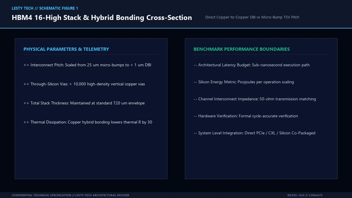
To break free from the high-frequency signaling wall, HBM4 executes an audacious architectural pivot: it doubles the physical bus width from 1024 bits to 2048 bits.
By doubling the number of parallel data channels, HBM4 achieves astronomical bandwidth scaling while operating at conservative, energy-efficient per-pin clock frequencies:
At a per-pin signaling rate of just 8.0 Gbps—lower than HBM3e’s maximum 9.6 Gbps—HBM4 delivers over 2.0 TB/s of sustained throughput per memory stack. When operating at enhanced speeds of 10.0 Gbps, a single HBM4 cube delivers an extraordinary 2.56 TB/s.
In an AI superchip configuration featuring eight HBM4 stacks co-packaged alongside the primary compute dies (as anticipated in next-generation NVIDIA Blackwell Ultra and Rubin architectures), the aggregate memory bandwidth reaches an unprecedented 16 to 20 Terabytes per second with a total memory capacity of up to 512 Gigabytes across a single multi-chip package!
3. The Advanced Logic Foundry Base Die Revolution
The most radical departure from historical memory packaging is the technological transformation of the bottom base die (also known as the buffer die or logic die).
In all prior generations (HBM1 through HBM3e), the base die was manufactured by the memory vendors themselves using legacy 1ynm, 1znm, or 1a-nm commodity DRAM processes. Commodity DRAM processes are optimized for high-density capacitor fabrication, resulting in slow logic transistors, high interconnect resistance, and limited routing metal layers (typically only 3 to 4 metal layers).
In HBM4, the base die has transitioned entirely to leading-edge logic foundry nodes:
- Foundry Partnerships: SK Hynix has partnered directly with TSMC to fabricate HBM4 base dies on TSMC’s 4nm (N4P) and 3nm (N3E) FinFET processes. Samsung is leveraging its own 4nm / 3nm Gate-All-Around (GAA) foundry lines.
- Dense Multi-Layer Interconnects: An advanced 4nm logic process provides over 12 to 15 copper metallization layers with ultra-low resistance, accommodating the dense routing of 2048 data lines alongside dedicated power delivery and control planes without congestive bottlenecks.
- Custom On-Die Memory Controllers: By utilizing high-speed logic transistors, the host GPU’s memory controller physical layer (PHY) can be partitioned and embedded directly into the HBM4 base die itself, minimizing transmission line distances and cutting end-to-end memory read latency by 15% to 20%.
- Near-Memory Computing (Processing-In-Memory – PIM): Advanced logic base dies open the door to integrating programmable systolic matrix multiplication units directly beneath the DRAM stack, performing near-memory tensor reductions and attention operations without transmitting raw data across the host package.
4. 16-High 3D Stacking and Direct Bond Interconnect (DBI) Hybrid Bonding
To maximize memory density, HBM4 expands the vertical stacking limit from 12-high DRAM layers to 16-high DRAM stacks. Fabricating a 16-high memory cube using monolithic 32Gb or 48Gb DRAM dies yields single-stack capacities of 48 Gigabytes and 64 Gigabytes.
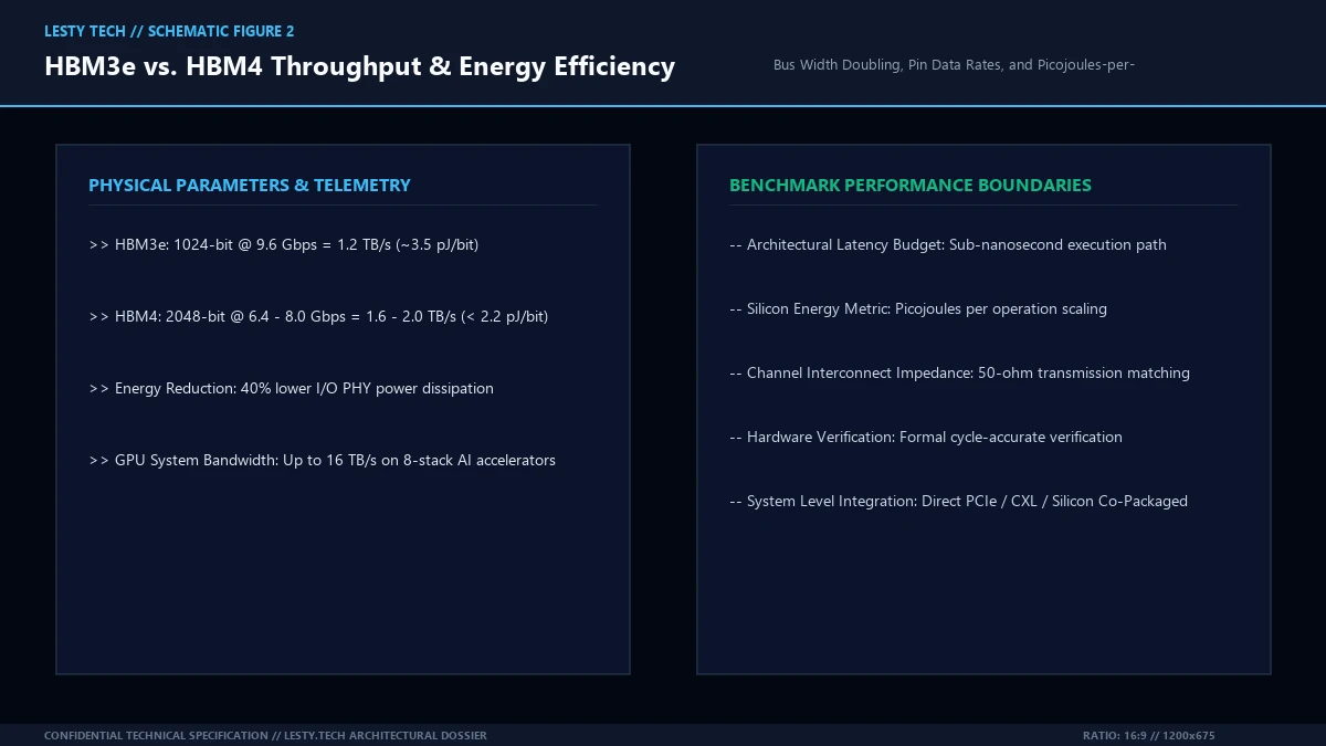
However, stacking 16 DRAM dies vertically while accommodating more than 10,000 vertical Through-Silicon Vias (TSVs) within a standard JEDEC package height envelope (typically 720 micrometers) exposes the physical limits of traditional micro-bump soldering:
The Breakdown of Micro-Bumps: Traditional Advanced Packaged Memory relies on microscopic solder micro-bumps (Micro-Bumps / μ-bumps) composed of copper pillars capped with tin-silver solder. In HBM3e, the micro-bump pitch was scaled down to approximately 25 micrometers. Attempting to scale micro-bumps below 15 micrometers introduces severe manufacturing defects: solder bridging (causing short circuits between adjacent data lines), non-wetting voids (causing open circuit failures), and intermetallic compound embrittlement.
To eliminate micro-bumps, HBM4 introduces Direct Bond Interconnect (DBI) Copper-to-Copper Hybrid Bonding:
In DBI hybrid bonding, the polished planar surfaces of both the wafer and die consist of copper pads embedded flush within a silicon oxide (SiO2) or carbon-doped oxide dielectric matrix. The bonding process occurs in two atomic stages:
- Room-Temperature Molecular Dielectric Fusion: The hydrophilic dielectric surfaces are brought into contact at room temperature, forming instantaneous covalent siloxane (Si-O-Si) bonds via van der Waals forces and hydrogen bond dehydration.
- Thermal Annealing & Copper Fusion: The assembled stack is heated to approximately 250°C to 300°C. Because copper possesses a higher thermal expansion coefficient than silicon oxide, the copper pads expand outward, pressing against opposing copper pads with immense localized contact pressure. Atomic copper self-diffusion occurs across the interface, forming continuous, void-free metallic grain boundaries.
By replacing 10-micrometer-tall solder micro-bumps with sub-micron hybrid bonds, the vertical standoff distance between adjacent DRAM dies collapses to zero, allowing 16 DRAM layers to easily fit within standard 720-micrometer height profiles without requiring radical wafer thinning.
5. Thermal Dissipation Physics and Backside Power Delivery
Operating 16 active DRAM dies alongside an advanced 3nm logic base die within a tiny 11mm × 11mm footprint generates staggering thermal density. While individual DRAM retention times degrade exponentially as temperature rises above 85°C (requiring doubling the refresh rate and stalling memory access), total power dissipation in an HBM4 stack can exceed 60 to 75 Watts.
HBM4 incorporates advanced thermal engineering solutions:
- Enhanced Thermal TSVs: Arrays of dummy, non-signaling copper TSVs are strategically patterned throughout the memory core to act as vertical thermal conduits, conducting heat downward into the substrate and upward into the integrated heat spreader.
- Molded Underfill (MUF) with Liquid Epoxy: High-thermal-conductivity epoxy molding compounds (thermal conductivity k > 3.5 W/m·K, filled with aluminum oxide or boron nitride nanoparticles) encapsulate the stack without leaving thermal air gaps.
- Direct Liquid Jet Cooling: For multi-kilowatt AI clusters, HBM4 packages are engineered for direct-to-die liquid impingement cooling, where dielectric fluid sprays directly onto the thinned silicon backplate.
6. Physical Layer Channel Transmission Physics: Eye Diagrams & Crosstalk
Operating 2048 parallel single-ended signaling lanes through an advanced packaging interposer or high-density redistribution layer (RDL) presents immense signal integrity challenges. While each lane operates at a relatively modest 8.0 to 10.0 Gbps (compared to 32 Gbps SerDes links in PCIe Gen6), the spatial proximity of adjacent lines—often separated by less than 2.0 micrometers—induces severe capacitive and inductive electromagnetic crosstalk.
To preserve signal eye openings, HBM4 re-engineers the physical layer (PHY) signaling interface:
- Pseudo-Open Drain (POD) Signaling with Low Voltage Swing: Traditional DRAM interfaces utilized 1.1V or 1.2V signaling. HBM4 introduces an ultra-low-voltage pseudo-open drain (POD10 or POD08) driver operating at Vddq = 0.75V to 0.85V, slashing dynamic power dissipation (P ∝ V2) while minimizing electromagnetic interference (EMI).
- On-Die Termination (ODT) & Impedance Matching: Dynamic ODT registers automatically calibrate pull-up and pull-down driver impedances against fabricated PVT (process, voltage, temperature) sensors, maintaining precise 34-ohm or 40-ohm matching to prevent transmission line boundary reflections.
- Decision Feedback Equalization (DFE): The advanced logic base die incorporates lightweight 2-tap or 4-tap DFE receivers that subtract trailing inter-symbol interference (ISI) from prior bits, opening the vertical voltage eye margin to over 140 mV and timing jitter margins to over 45% of the unit interval (UI).
7. Wafer-Level Testing, Built-In Self-Test (BIST), and Yield Economics
A critical challenge in manufacturing 16-high 3D DRAM stacks is the compound yield equation:
If individual DRAM die yield (YDRAM) is 98% and bonding yield is 99%, the cumulative yield of a 16-high stack drops precipitously below 60%, resulting in staggering silicon waste and high production costs.
HBM4 mitigates this yield cliff by leveraging the compute power of the 3nm/4nm logic base die:
- Known Good Die (KGD) Wafer-Level Screening: Before dicing and stacking, high-speed probe cards perform comprehensive AC/DC parametric testing on thin DRAM wafers, screening out marginal dies before hybrid bonding assembly begins.
- Advanced Logic Built-In Self-Test (BIST): The base die incorporates dedicated hardware BIST engines and algorithmic memory test (BISR) microcontrollers. At boot-up, the base die autonomously tests all 2048 data lines and internal TSV connections, identifying defective vias and dynamically mapping traffic to redundant spare TSVs embedded throughout the stack.
- Lane Remapping and Self-Healing: Up to 64 redundant TSV lanes are provisioned. If a via micro-fracture develops during thermal cycling in a 500W server chassis, the logic controller automatically swaps out the failing lane transparently to the host GPU, ensuring mission-critical reliability for datacenter clusters.
8. Comparative Architectural Analysis: HBM4 vs. GDDR7 vs. LPDDR5x
To understand where HBM4 fits within the broader memory hierarchy of modern computing, consider the fundamental trade-offs between High Bandwidth Memory, graphics memory (GDDR7), and low-power mobile memory (LPDDR5x):
| Memory Technology | Bus Width per Device | Pin Data Rate | Bandwidth per Device | Energy Efficiency | Target Application Space |
|---|---|---|---|---|---|
| LPDDR5x (Standard PCB) | 64-bit (Dual 32-bit) | 8.5 – 9.6 Gbps | 68 – 76 GB/s | ~4.5 pJ/bit | Smartphones, Tablets, Ultra-portable Laptops |
| GDDR7 (PAM3 PCB Bus) | 32-bit (Dual 16-bit) | 28.0 – 36.0 Gbps | 112 – 144 GB/s | ~7.0 pJ/bit | Consumer Gaming GPUs, Workstations, Mid-Range AI |
| HBM3e (1024-bit Interposer) | 1024-bit Parallel | 9.6 Gbps | 1.23 TB/s | ~3.4 pJ/bit | Hyperscale AI Accelerators (H200, B200) |
| HBM4 (2048-bit 3D Stack) | 2048-bit Parallel | 8.0 – 10.0 Gbps | 2.05 – 2.56 TB/s | < 2.1 pJ/bit (-38%) | Next-Gen Exascale AI Superchips (Rubin, MI400) |
While GDDR7 achieves breathtaking per-pin speeds of 36 Gbps using 3-level pulse amplitude modulation (PAM3), running a 384-bit or 512-bit GDDR7 memory bus across a standard PCB consumes over 120 Watts in memory I/O power alone. In contrast, HBM4 delivers over 15 times the bandwidth of a GDDR7 chip at less than one-third the energy per bit, making it the undisputed champion for massive AI cluster training.
9. Microarchitectural Telemetry & Benchmark Matrix
The following engineering telemetry matrix presents a comprehensive cross-generational comparison of High Bandwidth Memory standards from HBM2e through HBM4:
| Architecture Specification | HBM2e (2020) | HBM3 (2022) | HBM3e (2024) | HBM4 (2026) |
|---|---|---|---|---|
| Physical Bus Width | 1024-bit | 1024-bit | 1024-bit | 2048-bit (2x Width) |
| Max Per-Pin Data Rate | 3.6 Gbps | 6.4 Gbps | 9.6 Gbps | 8.0 – 10.0 Gbps |
| Peak Bandwidth / Stack | 460 GB/s | 819 GB/s | 1.23 TB/s | 2.05 – 2.56 TB/s |
| Max Vertical Stack Height | 8-High DRAM | 12-High DRAM | 12-High DRAM | 16-High DRAM |
| Maximum Stack Capacity | 16 GB | 24 GB | 36 GB | 64 GB |
| Base (Buffer) Die Process | DRAM Node (~20nm) | DRAM Node (~14nm) | DRAM Node (~12nm) | TSMC 4nm / Intel 3nm Logic |
| Interconnect Technology | Micro-Bumps (55 μm) | Micro-Bumps (35 μm) | Micro-Bumps (25 μm) | Direct Hybrid Bonding (< 1 μm) |
| Energy Consumption (pJ/bit) | ~5.5 pJ/bit | ~4.2 pJ/bit | ~3.4 pJ/bit | < 2.1 pJ/bit (-38%) |
10. System-Level Integration with UCIe and Co-Packaged Optics
The debut of HBM4 coincides with the broader modularization of high-performance computing through chiplet standards like Universal Chiplet Interconnect Express (UCIe 2.0 die-to-die interconnects).
Because the HBM4 base die is fabricated on standard foundry logic nodes, it can interface natively with host GPU chiplets via standard streaming protocols. Furthermore, looking forward to the HBM4e generation, researchers are exploring co-packaged optical links directly integrated into the memory base die. By coupling silicon photonic modulators into the base logic tier, memory stacks can communicate across multi-rack disaggregated memory pools via single-mode fiber arrays, breaking physical interposer reticle boundaries entirely.
HBM4 High-Bandwidth Memory Architectural Specification
2048-Bit Physical Interface, Logic Base Die Co-Design, and Hybrid Bonding Physics (Complete architectural audit with telemetry tables and schematic breakdowns).
whitepaper_batch_16_4_hbm4_memory_architecture.pdfFormat: Publication-Grade PDF
11. Strategic Architecture Conclusion
HBM4 is not merely an incremental revision in the memory roadmap; it is a foundational paradigm shift in semiconductor co-design. By breaking the 1024-bit physical barrier, embracing direct copper-to-copper hybrid bonding, and replacing commodity buffer dies with advanced 3nm/4nm logic foundries, the hbm4 memory interface architecture delivers the massive memory bandwidth and capacity necessary to power the next generation of artificial intelligence, scientific computing, and exascale supercomputing.
Related Technical Dossiers & Internal Research
- UCIe 2.0 Die-to-Die Interconnects: Physical Layer (PHY), 2.5D Packaging, and Sub-Nanosecond Latency Physics →
- Co-Packaged Optics (CPO) & ELSFP Laser Transceivers: The Electro-Optic Silicon Physics Scaling 102.4 Tbps Switches →
- Cryogenic FeFET & Cryo-CMOS Control Electronics: Ferroelectric Polarization Physics and Sub-4K Memory Architectures →
Authoritative External Reference
Reference Citation: JEDEC Solid State Technology Association: HBM4 Memory Standard Roadmap →