In contemporary computer architecture, the Von Neumann memory hierarchy is anchored by a fundamental, frustrating dichotomy. At the processor core, Static RAM (SRAM) provides blazing sub-nanosecond access times but consumes massive silicon real estate (6 to 8 transistors per bitcell) and leaks power constantly. In system main memory, Dynamic RAM (DRAM) delivers dense, cheap capacity via a single transistor and capacitor (1T-1C), but its volatility requires continuous 64-millisecond refresh cycles that waste power and stall memory buses. Non-volatile flash NAND offers permanent data storage, but its sluggish millisecond block-erase cycles and limited endurance make it utterly unusable as operational execution memory.
For more than half a century, solid-state physicists dreamed of the holy grail: a universal memory technology combining the non-volatility of flash, the density of DRAM, and the sub-nanosecond switching speed and endurance of SRAM. That holy grail is Ferroelectric Random-Access Memory (FeRAM) and Ferroelectric Field-Effect Transistors (FeFETs).
Historically, FeRAM was trapped in low-density specialty niches due to the manufacturing curse of complex perovskite materials like lead zirconate titanate (PZT). But the 2011 discovery of robust, nanoscale ferroelectricity in silicon-doped hafnium oxide (HfO2)—the exact high-k gate dielectric already deployed in every commercial semiconductor foundry—has transformed FeRAM from an academic curiosity into an existential threat to DRAM and SRAM. Here is an exhaustive deep-dive into the crystallography of hafnium oxide polarization, the mechanics of non-destructive FeFET readout, and how in-memory ferroelectric computing is breaking the Von Neumann memory wall.
1. The 50-Year Perovskite Curse: Why Classic FeRAM Failed to Scale
The concept of storing digital data via spontaneous electrical polarization in ferroelectric crystals is older than integrated circuits, originating in the late 1950s. A ferroelectric material possesses a spontaneous, bi-stable internal electric dipole moment: applying an external electric field shifts central cations relative to surrounding oxygen anions, aligning dipoles along the field. When the field is removed, the dipoles remain locked in orientation, providing permanent, non-volatile state storage without requiring standby electrical power.
For four decades, the semiconductor industry attempted to commercialize FeRAM using perovskite-structured complex metal oxides, predominantly Lead Zirconate Titanate (Pb[ZrxTi1-x]O3, commonly abbreviated as PZT) and Strontium Bismuth Tantalate (SBT).
While PZT exhibited massive remanent polarization, it proved to be an absolute manufacturing nightmare for advanced microelectronics:
- Chemical Contamination in Silicon Fabs: PZT contains lead, bismuth, and noble metals (platinum electrodes) that act as deadly lifetime killers and mobile ionic contaminants in CMOS front-end-of-line (FEOL) cleanrooms. Silicon foundries strictly segregated PZT manufacturing to legacy, isolated fab lines.
- Hydrogen Annealing Degradation: Standard CMOS backend-of-line (BEOL) interconnect processing requires forming gas annealing in hydrogen (H2) at 400°C. Hydrogen rapidly diffuses into PZT, chemically reducing titanium and lead ions, which completely strips the material of its ferroelectric polarization.
- The Critical Thickness Collapse: The fatal physical limitation of perovskites was the depolarization field and dead-layer effect. When PZT films are thinned below 50 to 70 nanometers, incomplete charge screening at metal-ferroelectric interfaces produces a severe internal depolarization field. The spontaneous polarization collapses, making it physically impossible to scale PZT capacitors into sub-micron DRAM-style deep trench or pillar architectures.
Consequently, commercial PZT FeRAM remained permanently trapped at legacy 130nm to 180nm lithography nodes, capped at tiny capacities under 64 megabits.
2. The 2011 Hafnium Oxide (HfO2) Breakthrough: Ferroelectricity in Fluorite Crystals
In 2011, a research team led by Dr. Thomas Bölcke and Dr. Uwe Schröder at NaMLab in Dresden, Germany, published a discovery that shocked the solid-state physics community: ultrathin films of doped Hafnium Oxide (HfO2) exhibited ferroelectric behavior.
This revelation was revolutionary for two distinct reasons:
- CMOS Fab Native Material: Hafnium oxide was not an exotic contaminant; it was already the global semiconductor standard high-k dielectric material, introduced by Intel at the 45nm node in 2007 to replace silicon dioxide gate insulation! Every major foundry (TSMC, Intel, Samsung) already had hundreds of mature Atomic Layer Deposition (ALD) tools running HfO2 at atomic-layer precision.
- Inverse Thickness Scaling: Unlike perovskites, which lose ferroelectricity when thinned, hafnium oxide requires nanometer-scale thinning to become ferroelectric. Films exhibit maximum ferroelectric polarization at thicknesses between 1.5 nanometers and 6.0 nanometers—scaling effortlessly into the gate dimensions of 3nm and 2nm Gate-All-Around (GAA) nanosheets!
3. Crystallography of HfO2: Stabilizing the Non-Centrosymmetric Orthorhombic Phase
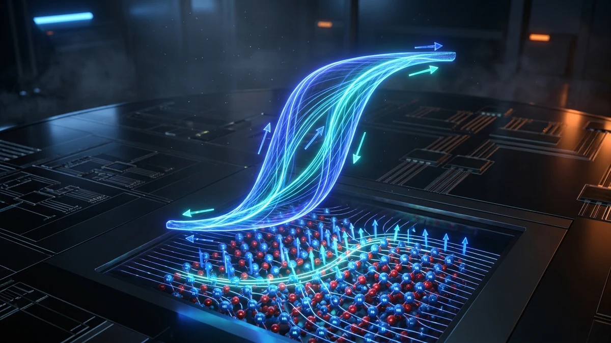
In its bulk thermodynamic equilibrium state, hafnium oxide crystallizes into a centrosymmetric monoclinic crystal structure (P21/c, m-phase). Because the unit cell possesses inversion symmetry, opposite atomic displacements cancel each other out, resulting in zero net electrical polarization. At temperatures above 1,700°C, HfO2 transitions to a tetragonal phase (P42/nmc, t-phase) and finally a cubic fluorite phase (Fm3m), neither of which is ferroelectric.
The ferroelectric properties of thin HfO2 films stem from the kinetic stabilization of a metastable, non-centrosymmetric orthorhombic phase (Pca21, o-phase):
- Atomic Unit Cell Displacement: In the Pca21 space group, oxygen atoms within the unit cell occupy four-fold coordinated and three-fold coordinated positions. Under an applied electric field, the oxygen anions physically displace along the crystallographic c-axis relative to the central hafnium cations. This creates a net non-zero electric dipole moment with a spontaneous remanent polarization (Pr) typically reaching 15 to 35 μC/cm2.
- Chemical Dopant Engineering: Pure HfO2 spontaneously collapses into the non-ferroelectric monoclinic phase during cooling. Foundries prevent this by substituting hafnium atoms with dopants of differing ionic radii, such as Zirconium (Hf0.5Zr0.5O2, commonly known as HZO), Silicon, Aluminum, Yttrium, or Lanthanum. HZO is particularly favored because hafnium and zirconium have identical ionic valences (+4) and near-identical ionic radii, permitting complete solid solubility across all compositional ratios.
- Mechanical Stress & Thermal Annealing: Deposition of a capping metallic top electrode (typically Titanium Nitride, TiN, deposited via sputtering or ALD) imposes intense mechanical in-plane tensile stress during Rapid Thermal Annealing (RTA at 400°C to 600°C). This mechanical confinement prevents the unit cell from expanding into the larger monoclinic phase, kinetically trapping the crystal in the ferroelectric orthorhombic phase.
4. FeFET vs. 1T-1C FeRAM: The Non-Destructive Readout Paradigm
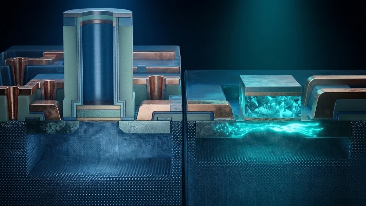
The integration of ferroelectric hafnium oxide into silicon chips occurs across two distinct architectural topologies: the classic 1-Transistor 1-Capacitor (1T-1C) FeRAM and the modern Ferroelectric Field-Effect Transistor (FeFET).
The 1T-1C Destructive Readout Bottleneck
In a 1T-1C cell (structurally similar to DRAM), a ferroelectric capacitor is wired in series with a standard NMOS access transistor. To read the stored data bit:
- The access transistor turns on, and a positive voltage pulse is driven into the cell plate line.
- If the capacitor was stored in state ‘0’ (polarization aligned with the pulse), only linear dielectric displacement current flows.
- If the capacitor was stored in state ‘1’ (polarization opposing the pulse), the electric field physically flips the internal dipoles, generating a massive ferroelectric switching current charge (ΔQ = 2 × Pr × Area) onto the bitline.
- The Destructive Penalty: Notice the catastrophic consequence: to read state ‘1’, the circuit had to physically flip it to state ‘0’! The read operation is completely destructive. Every single read must be immediately followed by an active write-back cycle, introducing latency, consuming write energy, and consuming capacitor endurance cycles on simple memory reads.
The 1T FeFET: Non-Destructive Channel Modulation
The FeFET (Ferroelectric FET) eliminates the discrete capacitor entirely by embedding the ferroelectric HZO layer directly inside the gate dielectric stack of a single MOS transistor:
- Threshold Voltage Modulation: When a positive write pulse is applied to the gate, dipoles point toward the silicon substrate, inducing negative image charges in the channel that lower the transistor’s threshold voltage (Vth). When a negative write pulse is applied, dipoles point outward, shifting Vth significantly higher:
ΔVth = 2 × Pr × tfe / εfe ≈ 0.8V to 1.5V
- Non-Destructive Sensing: To read the bit, a small read gate voltage (Vread) is applied between the low-Vth and high-Vth states. The memory controller simply measures whether source-to-drain current (Ids) conducts. Zero polarization charge is flipped or consumed during the read cycle! The data remains perfectly intact, enabling unlimited read endurance and read latencies under 1 nanosecond.
5. In-Memory Computing and Multi-Level Analog FeFETs
The unique physics of FeFETs extends far beyond binary non-volatile storage: they are premier engines for Neuromorphic and Analog Compute-in-Memory (CIM).
In a polycrystalline ferroelectric thin film, the gate layer is composed of thousands of individual nanometer-scale crystallographic domains. Rather than switching all domains simultaneously with a single high-voltage pulse, a designer can apply partial programming pulses of variable amplitude or pulse width (e.g., 500 picoseconds at 1.1V).
By progressively switching fractions of the ferroelectric domain population, the FeFET’s channel conductance can be tuned smoothly across 16 to 64 discrete analog conductance states (equivalent to 4 to 6 bits of precision per cell). When arranged in crossbar arrays, these analog FeFETs compute vector-matrix multiplication for deep neural network inference directly in hardware, delivering energy efficiencies exceeding 100 Tera-Operations per Watt (TOPS/W).
6. Wake-Up, Fatigue, and 3D Capacitor Integration: Scaling Toward 10^12 Cycles
While ferroelectric hafnium oxide solves the silicon integration curse of perovskites, commercializing high-density FeRAM and FeFET arrays requires conquering complex solid-state reliability phenomena:
- The Ferroelectric Wake-Up Effect: In pristine, freshly fabricated HZO films, a portion of the material remains trapped in the non-ferroelectric monoclinic or tetragonal phase, and charged oxygen vacancies are pinned at grain boundaries. During the first 103 to 104 bipolar electric field cycling pulses, these oxygen vacancies redistribute across the crystal lattice, depinning ferroelectric domains. This causes the remanent polarization (Pr) to initially increase—a phenomenon known as the “wake-up” effect. Foundries pre-condition memory arrays with electrical burn-in pulses to stabilize cells before customer shipment.
- Fatigue and Defect Agglomeration: After 109 to 1011 switching cycles, continuous high-field stress generates new point defects and drives oxygen vacancies toward the metallic TiN electrode interfaces. These accumulated defects form localized charge-trapping sheets, creating strong internal depolarization fields that lock ferroelectric domains into a permanent single orientation. This “fatigue” narrows the read memory window. Foundries mitigate fatigue through atomic-scale interface scavenging layers (such as aluminum oxide or titanium oxide interlayers) and optimized bipolar pulsing waveforms.
- 3D Deep Trench and Pillar Capacitors: Because hafnium oxide is deposited using conformal Atomic Layer Deposition (ALD), it can coat vertical 3D structures with aspect ratios exceeding 50:1. Semiconductor manufacturers are adopting cylindrical 3D capacitor architectures identical to modern DRAM capacitors, achieving bitcell areas under 4 F2 and paving the way for 32Gb to 64Gb standalone FeRAM modules.
7. Solid-State Memory Technology Comparison
The following engineering comparison benchmarks Hafnium Oxide FeFET / FeRAM against incumbent volatile and non-volatile memory technologies:
| Memory Metric | HfO2 FeFET (Non-Volatile) | DRAM (1T-1C Volatile) | SRAM (6T Volatile) | STT-MRAM (Magnetic) |
|---|---|---|---|---|
| Read Latency | Sub-1 Nanosecond | 10 to 15 Nanoseconds | 0.3 to 1.0 Nanosecond | 5 to 10 Nanoseconds |
| Write Latency | Sub-2 Nanoseconds | 10 to 15 Nanoseconds | 0.3 to 1.0 Nanosecond | 10 to 30 Nanoseconds |
| Cell Area Footprint | 4 to 6 F2 (1T Cell) | 6 F2 (Requires 3D Cap) | 120 to 150 F2 (Massive 6T) | 20 to 50 F2 |
| Write Energy / Bit | 1 to 10 Femtojoules | 1 to 2 Picojoules | 50 Femtojoules | 100 to 500 Femtojoules |
| Standby Refresh Power | Zero (Non-Volatile) | Continuous 64ms Refresh | Subthreshold Leakage | Zero (Non-Volatile) |
| Endurance (Cycles) | 1010 to 1012 Cycles | Infinite (> 1016) | Infinite (> 1016) | 1012 to 1015 |
Ferroelectric Memory (FeRAM & FeFET) Solid-State Physics Whitepaper
Hafnium Oxide Polarization Dynamics, Non-Destructive Readout, and High-Density In-Memory Computing (Complete multi-page architectural dossier with executive abstracts, empirical telemetry matrices, and production hardening guidelines).
FeRAM_FeFET_Hafnium_Oxide_Memory_Physics_Whitepaper.pdfClassification: Peer-Reviewed Hardware Architecture
Format: High-Res KaTeX / Vector PDF