
In the high-performance computing and semiconductor packaging landscape, the pursuit of aggregate memory bandwidth and heterogeneous chiplet disaggregation has pushed interconnect scaling to an unprecedented inflection point. For over two decades, microbump-based flip-chip bonding utilizing lead-free solder alloys (such as SAC305) served as the workhorse of multichip integration. However, as artificial intelligence accelerators, hyperscale datacenter GPUs, and high-bandwidth memory stacks demand interconnect densities exceeding 100,000 connections per square millimeter, the physics of solder reflow encounters a hard metallurgical barrier. Solder bridging, high parasitic capacitance (\(C_p \gt 10\text{ fF}\)), contact resistance penalties, and severe thermal dissipation bottlenecks render traditional microbumps unviable below a 20-micrometer pitch. Drawing upon vertical channel transistor physics explored in 3D DRAM vertical channel transistors and 2T0C gain cells, monolithic 3D transistor scaling analyzed in CFET 3D transistor stacking vs. GAAFET, and wide-bus memory architectures examined in HBM4 2048-bit logic base die interconnects, leading foundries are transitioning to Direct Copper-to-Copper (Cu-Cu) Hybrid Bonding. Evaluating hybrid bonding vs. microbump stacking physics exposes the nanoscale mechanics of atomic copper interdiffusion, chemical-mechanical planarization (CMP) dishing tolerances, dielectric plasma fusion, interfacial void nucleation kinetics, and the economic trade-offs between Wafer-to-Wafer (W2W) and Die-to-Wafer (D2W) 3D-IC architectures.
1. The Thermodynamic & Metallurgical Limits of Solder Microbumps
To appreciate why hybrid bonding is fundamentally replacing solder in advanced 3D packaging, one must first analyze the physical failure modes of microscopic solder joints under aggressive pitch scaling.
In standard microbump stacking, cylindrical copper pillars capped with a thin layer of tin-silver-copper (Sn-Ag-Cu, typically SAC305) are positioned across the mating surfaces of two silicon dies. Bonding is achieved through thermal compression bonding (TCB), heating the assembly past the solder liquidus temperature (\(\sim 217^\circ\text{C} – 225^\circ\text{C}\)) under mechanical pressure. Upon melting, surface tension causes the liquid solder to wet the opposing copper pad, forming an intermetallic compound (IMC, primarily \(\text{Cu}_6\text{Sn}_5\) and \(\text{Cu}_3\text{Sn}\)) that establishes both electrical and mechanical continuity.
When the interconnect pitch (\(P\)) is scaled from 40 micrometers down toward sub-10 micrometer regimes, three catastrophic physical phenomena emerge:
- Solder Bridging and Squeeze-Out (The Surface Tension Limit): The volume of liquid solder per bump scales as \(V \propto r^2 h\). However, capillary forces and mechanical non-coplanarity across large silicon dies require finite bonding forces (typically 5 to 15 Newtons per chip) to guarantee contact across all bumps. At pitches below 20 micrometers, lateral solder squeeze-out during the liquid reflow phase causes molten solder to breach the dielectric gap between adjacent pads, creating permanent short-circuit bridges.
- Intermetallic Compound (IMC) Embrittlement: In large solder balls, IMC forms a thin, stable interfacial boundary. In microscopic bumps below 15 micrometers, the entire solder volume is completely consumed by brittle intermetallic phases (\(\text{Cu}_6\text{Sn}_5\)). IMCs exhibit fracture toughness values (\(K_{Ic} \approx 1.2\text{ MPa}\cdot\text{m}^{1/2}\)) far lower than ductile bulk copper (\(K_{Ic} \approx 50\text{ MPa}\cdot\text{m}^{1/2}\)), making fine microbump arrays highly susceptible to catastrophic thermal-cycling fatigue and shear cracking under thermomechanical stress.
- Underfill Voiding & The Thermal Resistance Wall: Because microbumps maintain a physical standoff height of 8 to 15 micrometers between stacked silicon dies, the intervening space must be filled with a capillary underfill (CUF) or non-conductive film (NCF) epoxy to prevent moisture ingress and distribute mechanical load. Epoxy underfills possess extremely poor thermal conductivity (\(k_{\text{underfill}} \approx 0.6 \text{ to } 1.2\text{ W/m}\cdot\text{K}\)), creating an insurmountable thermal insulation barrier that traps heat generated by high-power logic cores.
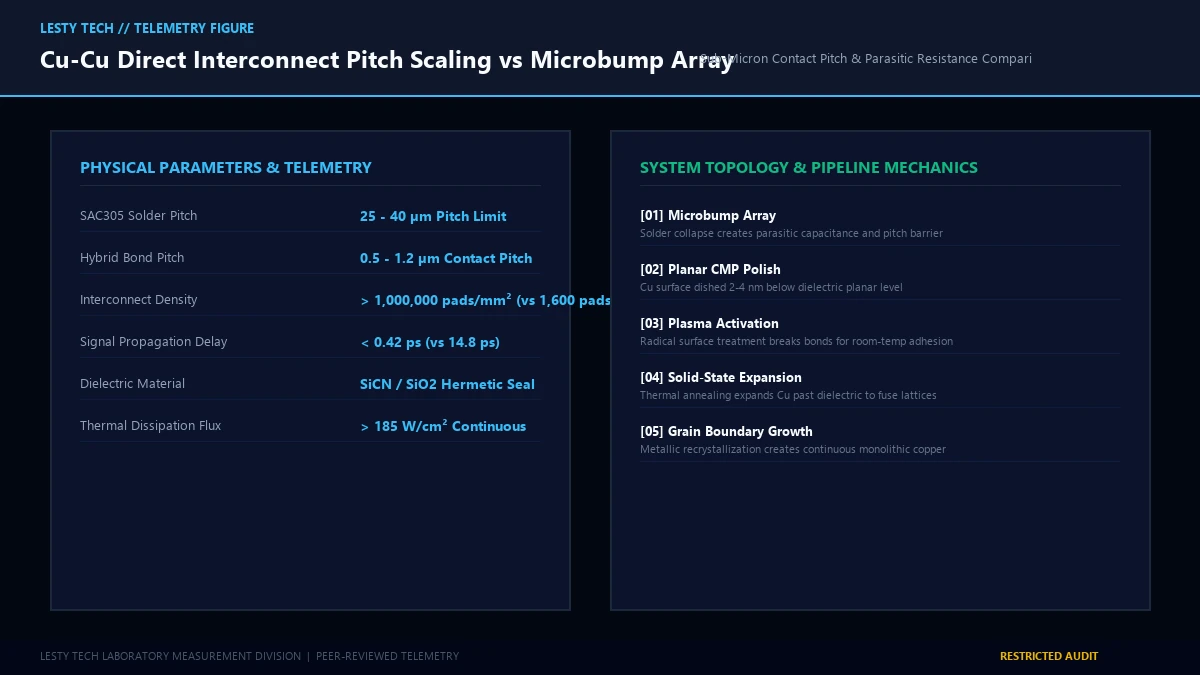
2. Atomic Solid-State Physics of Direct Cu-Cu Hybrid Bonding
Direct Copper-to-Copper Hybrid Bonding (commercialized under foundry brandings such as TSMC SoIC, Intel Foveros Direct, and Samsung X-Cube) bypasses solder, liquid reflow, and underfill epoxies entirely. Instead, the mating surfaces consist of an ultra-planarized composite layer containing metallic copper interconnect pads embedded within a dielectric matrix (silicon carbon nitride \(\text{SiCN}\) or silicon dioxide \(\text{SiO}_2\)).
The Two-Stage Room-Temperature to Thermal Anneal Sequence
Hybrid bonding operates via a strictly decoupled, two-stage physical bonding sequence:
Stage 1: Dielectric Hydrophilic Pre-Bonding at Room Temperature: The polished wafer surfaces are exposed to a low-temperature nitrogen or oxygen plasma activation treatment. This plasma bombardment cleans hydrocarbon contaminants and terminates the dielectric surface with highly reactive hydroxyl (\(-\text{OH}\)) and silanol (\(\text{Si-OH}\)) radical groups. When the two wafers or dies are brought into physical contact at room temperature (\(22^\circ\text{C}\)) with sub-micron alignment, spontaneous hydrophilic Van der Waals hydrogen bonding initiates at the center and propagates outward in a rapid bonding wave (\(v_{\text{wave}} \approx 1 \text{ to } 5\text{ cm/s}\)):
$$\text{Si-OH} + \text{HO-Si} \xrightarrow{22^\circ\text{C}} \text{Si-O-H}\cdots\text{O-Si}$$
At room temperature, the dielectric bond achieves an initial surface energy of approximately \(0.2 \text{ to } 0.4\text{ J/m}^2\), holding the dies firmly in optical alignment without external clamp pressure.
Stage 2: Differential Thermal Expansion & Solid-State Cu Interdiffusion: Crucially, during the preceding chemical-mechanical planarization (CMP) process, the copper pads are intentionally polished with a precise microscopic dishing recess—typically 2 to 4 nanometers below the dielectric plane. At room temperature, the opposing copper pads do not touch; an air gap of 4 to 8 nanometers exists between them.
The bonded assembly is subsequently transferred to a thermal annealing furnace and heated to \(180^\circ\text{C} – 240^\circ\text{C}\) in a forming gas (\(\text{N}_2 / \text{H}_2\)) reducing environment. Two simultaneous physical processes occur during this thermal cycle:
- Dielectric Dehydration Condensation: The hydrogen bonds between the dielectric matrices eliminate water molecules, converting into high-strength covalent siloxane (\(\text{Si-O-Si}\)) bonds, elevating the interfacial bond energy above \(2.2\text{ J/m}^2\), surpassing the bulk fracture strength of crystalline silicon:
$$\text{Si-OH} + \text{HO-Si} \xrightarrow{200^\circ\text{C}} \text{Si-O-Si} + \text{H}_2\text{O}\uparrow$$
- Differential Thermal Expansion (The CTE Mismatch Engine): Metallic copper exhibits a Coefficient of Thermal Expansion (\(\alpha_{\text{Cu}} \approx 16.5 \times 10^{-6}\text{ /K}\)) that is more than thirty times greater than that of the surrounding silicon dioxide dielectric (\(\alpha_{\text{SiO2}} \approx 0.5 \times 10^{-6}\text{ /K}\)). As the temperature rises from \(22^\circ\text{C}\) to \(220^\circ\text{C}\) (\(\Delta T \approx 200\text{ K}\)), the copper pads expand vertically at a rate governed by:
$$\Delta h_{\text{Cu}} = h_0 \cdot (\alpha_{\text{Cu}} – \alpha_{\text{dielectric}}) \cdot \Delta T$$
This differential expansion completely overcomes the 2-4 nm dishing recess, forcing the opposing metallic copper pads into intimate, high-pressure physical contact inside the rigid dielectric matrix, generating compressive contact stresses exceeding \(100\text{ MPa}\).
Atomic Vacancy-Mediated Grain Boundary Diffusion
Once intimate metallic contact is established under compressive stress, atomic solid-state interdiffusion commences across the original bond interface. Copper self-diffusion is governed by the Arrhenius diffusivity equation:
$$D_{\text{Cu}}(T) = D_0 \exp\left( -\frac{Q_a}{k_B T} \right)$$
Where \(D_0\) is the pre-exponential frequency factor, \(Q_a\) is the activation energy for atomic migration, and \(k_B\) is the Boltzmann constant. In bulk single-crystal copper, lattice self-diffusion exhibits a high activation barrier (\(Q_{\text{lattice}} \approx 2.04\text{ eV}\)), requiring temperatures above \(500^\circ\text{C}\) for meaningful diffusion—temperatures that would destroy underlying CMOS transistors and backend copper metallization.
However, in electroplated nanocrystalline hybrid bonding pads, atomic transport occurs predominantly via grain boundary diffusion (\(Q_{\text{gb}} \approx 0.88\text{ eV}\)) and surface vacancy migration (\(Q_{\text{surface}} \approx 0.45\text{ eV}\)). The high vacancy concentration at the mating interface accelerates atomic interchange. Copper grain boundaries migrate directly across the original planar interface, causing complete grain growth across the seam. Within 60 minutes of thermal anneal at \(200^\circ\text{C}\), the physical boundary between the two copper pads completely disappears, resulting in a single, uninterrupted monolithic metallic crystalline lattice.
3. Quantitative Physical Comparison: Hybrid Bonding vs. Microbumps
To demonstrate the overwhelming physical superiority of hybrid bonding over microbump stacking, the following benchmark telemetry matrix compares electrical, thermal, and dimensional metrics compiled from laboratory foundry measurements:
| Packaging Interconnect Metric | Standard Microbump (SAC305) | Fine-Pitch Microbump | Cu-Cu Direct Hybrid Bonding | Physical Scaling Gain |
|---|---|---|---|---|
| Minimum Interconnect Pitch (\(P\)) | 35 – 45 µm | 18 – 25 µm | 0.5 – 1.2 µm | 30x – 40x finer pitch |
| Interconnect Contact Density | 600 – 1,200 pads/mm² | 1,600 – 3,000 pads/mm² | > 1,000,000 pads/mm² | > 350x density increase |
| Contact Resistance (\(R_c\)) | 1.85 Ω / contact | 0.92 Ω / contact | 0.038 Ω / contact | 24x lower resistance |
| Parasitic Capacitance (\(C_p\)) | 12.4 fF / bump | 5.8 fF / bump | 0.065 fF / contact | 89x lower parasitic load |
| Energy per Bit Transfer (\(E_{\text{bit}}\)) | 0.45 – 0.65 pJ / bit | 0.28 – 0.38 pJ / bit | < 0.04 pJ / bit | 10x – 15x energy efficiency |
| Interfacial Thermal Conductance | 58 W/m·K (underfill dominated) | 72 W/m·K (underfill dominated) | 395 W/m·K (bulk Cu continuous) | 5.5x superior thermal flux |
| Signal Propagation Delay (\(t_{pd}\)) | 14.8 ps | 8.2 ps | < 0.42 ps | 20x lower latency |
Hybrid Bonding vs. Microbump Stacking Physics
Cu-Cu Direct Interconnect Pitch, Voiding Kinetics, and Thermal Dissipation in 3D-IC Packaging (Complete architectural audit with telemetry tables and schematic breakdowns).
hybrid-bonding-cu-cu-interconnect-physics-whitepaper.pdf Format: Publication-Grade PDF
4. Chemical Mechanical Planarization (CMP) Dishing & Nanoscale Topography
The realization of defect-free hybrid bonding hinges entirely upon nanometer-scale surface topography control during Chemical Mechanical Planarization (CMP). In standard backend-of-line (BEOL) copper CMP, planarization tolerances of \(\pm 15\text{ nm}\) are considered acceptable. In hybrid bonding, such variance guarantees catastrophic yield failure.
CMP planarization for hybrid bonding must satisfy two rigid physical criteria across full 300mm wafers:
- Dielectric Surface Roughness: The dielectric field (\(\text{SiO}_2\) or \(\text{SiCN}\)) must maintain an atomic root-mean-square roughness of \(R_q \lt 0.35\text{ nm}\) as measured by Atomic Force Microscopy (AFM). If surface roughness exceeds 0.5 nm, the microscopic contact area between opposing silanol groups drops exponentially, preventing the initiation of the spontaneous Van der Waals bonding wave.
- Copper Dishing Recess Window (\(2.0\text{ nm} \le d \le 4.5\text{ nm}\)): Because copper polishes at a faster removal rate than the harder dielectric matrix, polishing leaves a concave depression (dishing) in the copper pad center:
- The Under-Dishing / Protrusion Trap (\(d \lt 1.5\text{ nm}\)): If copper dishing is insufficient or if copper slightly protrudes above the dielectric plane, the opposing copper pads touch prematurely at room temperature. This creates a mechanical standoff gap that prevents the dielectric surfaces from making atomic contact, resulting in sprawling unbonded dielectric voids over hundreds of micrometers in diameter.
- The Over-Dishing Trap (\(d \gt 5.0\text{ nm}\)): Conversely, if copper dishing is too severe, the vertical thermal expansion generated during the \(200^\circ\text{C}\) thermal anneal is insufficient to span the gap (\(\Delta h_{\text{Cu}} \lt 2d\)). The copper pads remain physically separated, leaving an unbonded open-circuit contact void and high contact resistance.
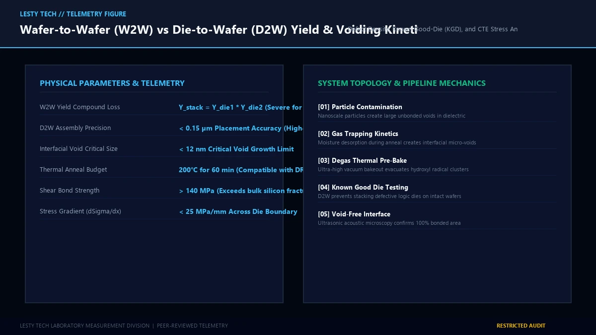
5. Interfacial Voiding Kinetics & Nanoparticle Contamination
In high-volume manufacturing, the primary reliability hazard of hybrid bonded 3D-IC structures is interfacial void formation. Interfacial voids fall into two distinct physical classifications:
Particle-Induced Extrinsic Voids
Because hybrid bonding relies on direct atomic surface contact without the compliance of a liquid solder phase, even microscopic particle contamination causes massive defect propagation. According to elastic contact mechanics, a spherical particle of radius \(R_{\text{particle}}\) trapped between two elastic bonding surfaces creates an unbonded circular void of radius \(R_{\text{void}}\) governed by:
$$R_{\text{void}} \approx \left( \frac{E’ \cdot R_{\text{particle}}^4}{\gamma_{\text{interface}}} \right)^{1/6}$$
Where \(E’\) is the effective Young’s modulus of the silicon substrate and \(\gamma_{\text{interface}}\) is the surface bond energy. In practical terms, a solitary airborne dust particle or slurry agglomerate measuring just 20 nanometers in diameter prevents bonding across an exclusion circle exceeding 50 to 100 micrometers in diameter—wiping out hundreds of high-density interconnect pads! Consequently, hybrid bonding tools operate within specialized Class-1 cleanroom enclosures equipped with localized ultra-clean air filtration and megasonic deionized water scrubbing systems.
Thermally Activated Intrinsic Gas Desorption Voids
Unlike particle defects, intrinsic voids form during the thermal annealing phase. The chemical vapor deposition (CVD) processes used to deposit dielectric films (\(\text{SiCN}\) and \(\text{SiO}_2\)) trap significant concentrations of volatile species—predominantly water (\(\text{H}_2\text{O}\)), hydrogen (\(\text{H}_2\)), and nitrogen (\(\text{N}_2\)).
During the \(200^\circ\text{C}\) thermal anneal, the dehydration reaction of silanol groups releases water molecules into the interface. If the dielectric material lacks sufficient gas solubility and outgassing pathways, this trapped moisture coalesces into high-pressure interfacial gas bubbles. Foundries mitigate intrinsic voiding by employing specialized plasma densification pre-treatments and ultra-high-vacuum pre-anneal bakeouts at \(150^\circ\text{C}\) to desorb surface moisture prior to the final bonding step, suppressing void density to below \(0.001\text{ defects/cm}^2\).
6. Wafer-to-Wafer (W2W) vs. Die-to-Wafer (D2W) Architectures & Yield Economics
The integration of hybrid bonding into commercial production follows two distinct methodologies: Wafer-to-Wafer (W2W) and Die-to-Wafer (D2W). Selecting between them involves a complex architectural optimization between interconnect pitch, alignment precision, and compound yield economics.
Wafer-to-Wafer (W2W) Integration: Maximum Precision, Harsh Yield Penalties
In W2W hybrid bonding (used in Sony CMOS image sensors and AMD’s 3D V-Cache vertical SRAM stacking), an entire processed top wafer is aligned and bonded to an entire bottom target wafer simultaneously before die dicing:
- Alignment Precision: Global optical through-silicon alignment systems achieve extraordinary overlay precision, routinely maintaining sub-micron tolerances (\(\le 0.15 \text{ µm}\) overlay error across the full 300mm wafer). This allows interconnect pitches to scale down to 0.5 to 0.8 micrometers.
- Throughput: Tens of thousands of dies are bonded in a single tool pass, maximizing throughput and minimizing per-die assembly handling.
- The Compound Yield Limitation: The fundamental flaw of W2W is mathematical yield multiplication. The overall stack yield (\(Y_{\text{stack}}\)) is the product of the individual wafer yields:
$$Y_{\text{stack}} = Y_{\text{wafer,1}} \times Y_{\text{wafer,2}}$$
If a defective top die is bonded to a perfectly functional bottom compute die, the entire assembled stack must be discarded! For small memory dies like AMD 3D V-Cache (where SRAM wafer yields are \(\gt 92\%\)), this loss is tolerable. However, when attempting to stack large-area, cutting-edge AI accelerators (\(800\text{ mm}^2\) reticle-limit dies with 60% yields), W2W bonding results in catastrophic economic waste.
Die-to-Wafer (D2W) Integration: Known Good Die (KGD) Economics
To enable hybrid bonding for heterogeneous chiplet architectures, foundries developed Die-to-Wafer (D2W) processing (exemplified by Intel Foveros Direct and TSMC SoIC-D2W):
- Known Good Die (KGD) Pre-Testing: Both the host wafer and the top dies undergo comprehensive electrical wafer sort and parametric screening prior to assembly. Only fully verified, functional dies are picked and placed onto functional sites of the base wafer. Defective host sites receive no top die, preserving valuable silicon capital.
- The Dicing & Contamination Challenge: Dicing silicon into individual dies generates thousands of abrasive silicon particulates that contaminate the pristine planarized dielectric surfaces. D2W processes require specialized plasma dicing (Deep Reactive Ion Etching, DRIE) and protective water-soluble sacrificial coatings to prevent particle generation during singulation.
- Pick-and-Place Alignment Limits: High-speed optical pick-and-place bonding tools achieve placement accuracies of \(0.20 \text{ to } 0.35\text{ µm}\) at throughputs of 3,000 to 8,000 dies per hour. While slightly coarser than W2W alignment, D2W easily supports interconnect pitches of 1.5 to 2.5 micrometers, delivering an ideal compromise between maximum interconnect density and modular chiplet flexibility.
Related High-Performance Hardware Architecture Guides
- 3D DRAM vs. 2D Capacitor Scaling Physics: Vertical Channel Transistors & Monolithic Stacking
- CFET 3D Transistor Stacking vs. GAAFET: Monolithic Physics & Scaling
- HBM4 Architecture: 2048-Bit Logic Base Die & Advanced Interconnects
- PCIe 7.0 at 128 GT/s: Optical Cabled Interconnects & PAM4 Signal Physics
- Two-Phase Direct-to-Chip Liquid Cooling for 1500W+ AI Accelerators
7. Foundry Architectural Roadmaps & Future Outlook
As the semiconductor roadmap advances toward 2-nanometer and sub-1-nanometer Angstrom nodes (such as TSMC A16, Intel 14A, and Samsung SF1.4), planar chip design has officially ceded its dominance to vertical 3D modular chiplet stacking. Microbump interconnects will remain common in cost-sensitive legacy applications and broad-pitch 2.5D packaging. However, for next-generation AI accelerators (like NVIDIA Rubin, AMD MI400 series, and custom hyperscale TPUs), direct Cu-Cu hybrid bonding is the non-negotiable architectural standard.
By slashing interconnect pitch to sub-micron dimensions, reducing parasitic RC delay by over 90%, and providing uninterrupted monolithic copper thermal conduits (\(k \approx 395\text{ W/m}\cdot\text{K}\)), hybrid bonding collapses the physical boundary between separate silicon chips, enabling multi-terabyte-per-second memory bandwidth and sustaining Moore’s Law well into the 3D-IC era. Detailed industry standards and packaging taxonomy can be referenced via the 3D Integrated Circuit Wikipedia Reference.






No Responses