
In the advanced semiconductor manufacturing and condensed matter physics landscape, the relentless scaling of silicon CMOS has reached an unforgiving physical frontier. For over five decades, Moore’s Law advanced primarily through planar lithographic shrinking, followed by the architectural transition to three-dimensional FinFETs at the 22nm node, and more recently, horizontal Gate-All-Around (GAAFET / nanosheet) transistors at the 3nm and 2nm nodes. However, as contacted poly pitch (CPP) drops below 40 nanometers and metal pitch shrinks below 20 nanometers, horizontal nanosheets encounter the “Standard Cell Height Wall.” Even with atomic-scale gate-all-around electrostatic control, standard logic cells remain bottlenecked by the mandatory lateral separation required between n-type (NMOS) and p-type (PMOS) sub-cells. Drawing upon fundamental semiconductor bandgap physics analyzed in MoS2 monolayer transistors and 2D semiconductors, wide-bandgap thermal dissipation examined in Diamond-on-GaN vs. GaN-on-SiC HEMT RF physics, and spintronic quantum transport in bismuth antimonide topological spintronics, the Complementary FET (CFET) has emerged as the definitive 3D monolithic device architecture for sub-1nm CMOS. Evaluating CFET 3D transistor stacking vs. GAAFET exposes the physics of vertical nanosheet epitaxy, Middle Dielectric Isolation (MDI), self-aligned contact etching, Backside Power Delivery Networks (BSPDN), and severe localized thermal dissipation bottlenecks.
1. The GAAFET Lateral Scaling Wall & Standard Cell Track Height Limits
To understand why semiconductor foundries are compelled to abandon horizontal GAAFET nanosheets at the sub-1nm frontier (the A14 and A10 nodes), one must analyze standard cell layout geometry and the electrostatic scaling equations governing nanoscale field-effect transistors.
In standard digital cell design, cell area (\(A_{\text{cell}}\)) is the product of Contacted Poly Pitch (CPP) and Cell Height (\(H_{\text{cell}}\)):
$$A_{\text{cell}} = \text{CPP} \times H_{\text{cell}} = \text{CPP} \times (N_{\text{tracks}} \times \text{MMP})$$
Where \(N_{\text{tracks}}\) is the cell track height (e.g., 6.0T, 5.0T, or 4.0T) and \(\text{MMP}\) is the Minimum Metal Pitch of the first interconnect metallization layer (Metal-0 or Metal-1). In horizontal GAAFET (such as Samsung MBCFET or Intel RibbonFET), nFET and pFET devices reside side-by-side on the planar substrate. Between the n-well and p-well regions lies a mandatory isolation trench known as the P-to-N boundary keep-out zone (\(W_{\text{iso}}\)):
$$H_{\text{cell}} = W_{\text{nFET}} + W_{\text{pFET}} + W_{\text{iso}} + 2 \times W_{\text{boundary}}$$
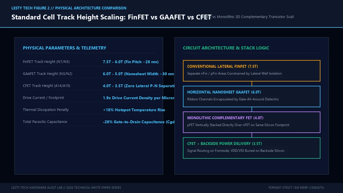
As foundries scaled from 5nm to 2nm, the contacted poly pitch contracted from 54nm to 45nm, and track heights were aggressive compressed from 7.5T down to 6.0T and 5.0T. However, at a 5.0T cell height, the physical width available for active nanosheet conduction channels (\(W_{\text{sheet}}\)) collapses below 25nm. If nanosheets are made too narrow, quantum confinement effects broaden the bandgap, scattering increases, and effective drive current per unit area (\(I_{\text{eff}}\)) plummets:
$$I_{\text{eff}} \approx \frac{1}{2} C_{\text{ox}} v_{\text{sat}} (V_{\text{DD}} – V_{\text{th}})^{\alpha}$$
Where \(C_{\text{ox}}\) is gate dielectric capacitance, \(v_{\text{sat}}\) is electron/hole saturation velocity, and \(\alpha\) is the velocity saturation index (\(1 \le \alpha \le 2\)). Because hole mobility in silicon (\(\mu_h \approx 450 \text{ cm}^2/\text{V}\cdot\text{s}\)) is inherently lower than electron mobility (\(\mu_e \approx 1400 \text{ cm}^2/\text{V}\cdot\text{s}\)), pFET channels require wider sheets or multiple stacked ribbons to match nFET drive currents. In a horizontal layout, widening pFET sheets forces the standard cell track height to expand, directly defying dimensional scaling.
Furthermore, scaling the lateral P-N spacing below 15nm induces severe dielectric breakdown, cross-diffusion of dopants during activation anneals, and extreme lithographic edge-placement errors (EPE). The semiconductor industry has reached an absolute lateral scaling wall: no further cell area reductions can be achieved while nFET and pFET devices reside side-by-side on the same silicon plane!
2. Monolithic vs. Sequential CFET: Vertical N-over-P Epitaxial Physics
The Complementary FET (CFET) solves this fundamental topological limit by folding the CMOS inverter into the third dimension. In a CFET architecture, nFET nanosheets are stacked directly above pFET nanosheets (or vice versa) on a single physical footprint, eliminating the lateral P-N separation zone entirely.
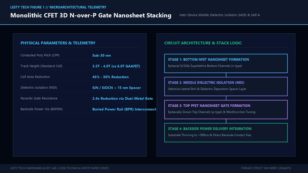
By collapsing the horizontal P-to-N keep-out distance to zero (\(W_{\text{iso}} \to 0\)), standard cell track height is reduced from 6.0T/5.0T down to 3.5T to 4.0T. A 4.0T CFET cell occupying a 30nm CPP achieves an immediate 45% to 50% cell-level area reduction compared to an optimized 2nm GAAFET cell, while simultaneously permitting wider nanosheet channels that boost active drive current.
In contemporary semiconductor research, two distinct physical integration paradigms exist for fabricating CFET devices: Monolithic CFET and Sequential CFET.
A. Monolithic CFET Integration
In Monolithic CFET, the entire multi-device vertical stack is fabricated on a single bulk silicon substrate through continuous epitaxial superlattice growth. An alternating superlattice composed of silicon (Si) and silicon-germanium (\(\text{Si}_{1-x}\text{Ge}_x\)) is epitaxially deposited:
$$\text{Substrate} \to [\text{SiGe} / \text{Si}]_n \ (\text{Bottom Channel}) \to \text{SiGe}_{\text{thick}} \ (\text{MDI Spacer}) \to [\text{SiGe} / \text{Si}]_p \ (\text{Top Channel})$$
Following high-aspect-ratio vertical fin patterning, isotropic chemical dry etching selectively removes the sacrificial \(\text{Si}_{1-x}\text{Ge}_x\) layers with extreme selectivity (\(> 150:1\)) relative to pure silicon. This leaves suspended silicon nanosheet ribbons for both the top and bottom devices. Key physical advantages of monolithic CFET include:
- Self-Aligned Precision: The top and bottom transistor channels are patterned simultaneously in a single lithographic exposure, eliminating layer-to-layer overlay errors (\(< 1 \text{ nm}\) misalignment).
- Standard Thermal Budgets: Dopant activation and gate dielectric formation follow established high-k metal gate (HKMG) processing sequences without risking wafer debonding.
- Substrate Cost Parity: Fabricated on standard bulk 300mm silicon wafers without requiring specialized donor/acceptor bonding carrier substrates.
B. Sequential CFET Integration
Sequential CFET (also referred to as 3D Monolithic or Layer Transfer CFET) fabricates the bottom transistor (typically nFET) on a primary host wafer through complete front-end-of-line (FEOL) processing. Subsequently, a thin crystalline layer of donor silicon or alternative channel material (e.g., Germanium or 2D transition metal dichalcogenides) is transferred and bonded to the host wafer via low-temperature direct oxide-oxide molecular bonding (\(\text{SiO}_2\text{-SiO}_2\)).
The top transistor (pFET) is then fabricated directly on top of the bonded layer. While sequential CFET allows the top and bottom channels to utilize completely different crystallographic orientations (e.g., \(\langle 100 \rangle\) for nFET electron mobility and \(\langle 110 \rangle\) for pFET hole mobility), it introduces severe engineering vulnerabilities:
- Thermal Budget Clamping: Because the bottom transistor and its metal interconnects already exist, all subsequent processing steps for the top transistor must remain strictly below 400°C to 450°C to prevent silicide agglomeration, gate dielectric crystallization, and dopant deactivation.
- Lithographic Overlay Misalignment: Wafer bonding distortion introduces 3-sigma overlay errors of 5nm to 10nm, completely destroying standard cell layout density benefits at sub-30nm contacted poly pitches.
Consequently, leading foundries—including TSMC (A14/A10), Intel (sub-RibbonFET nodes), and imec—have established Monolithic CFET as the primary manufacturing baseline for production sub-1nm CMOS.
3. Middle Dielectric Isolation (MDI) & Self-Aligned Contact (SAC) Physics
The single most demanding fabrication challenge in monolithic CFET engineering is the formation of the Middle Dielectric Isolation (MDI) layer and the self-aligned routing of electrical contacts between the vertically stacked nanosheets.
In a monolithic stack, the bottom nanosheets and top nanosheets are separated by a vertical distance of only 15 to 25 nanometers. Within this minuscule nanoscale gap, process engineers must deposit a robust, defect-free dielectric layer that satisfies three non-negotiable physical constraints:
- Zero Electrical Leakage: The isolation layer must withstand inter-device electric fields exceeding \(5 \text{ MV/cm}\) without dielectric breakdown or trap-assisted tunneling.
- Ultra-Low Parasitic Capacitance: The dielectric constant (\(k\)) must remain minimal (\(k < 5.0\)) to suppress inter-layer capacitive crosstalk between top and bottom gates. Materials such as carbon-doped silicon oxycarbide (SiOC) or silicon oxycarbonitride (SiOCN) are deposited via atomic layer deposition (ALD).
- Selective Chemical Stability: The MDI material must resist subsequent aggressive isotropic wet chemical etches and atomic vapor etching (ALE) sequences used to suspend the nanosheets and clean the gate trenches.
Following MDI formation, the system must establish separate electrical contact connections. Consider a CMOS inverter: the gates of the top pFET and bottom nFET must be electrically tied together (common input \(V_{\text{in}}\)), while their drain terminals must connect to form the common output (\(V_{\text{out}}\)). Conversely, the source of the top pFET must connect to \(V_{\text{DD}}\), while the source of the bottom nFET must connect to \(V_{\text{SS}}\) (Ground).
To wire these terminals without short-circuiting across the 15nm MDI boundary, foundries employ Self-Aligned Contact (SAC) etching and asymmetric dual-metal recess processes:
$$R_{\text{contact}} = \frac{\rho_c}{A_{\text{contact}}} + R_{\text{spreading}}$$
Where \(\rho_c\) is specific contact resistivity (\(\Omega\cdot\text{cm}^2\)) and \(A_{\text{contact}}\) is the physical interface area. At sub-1nm nodes, contact area drops below \(100 \text{ nm}^2\). To prevent \(R_{\text{contact}}\) from skyrocketing into the kilo-ohm regime, engineers deposit ultra-thin titanium silicide (\(\text{TiSi}_x\)) or nickel-platinum silicide (\(\text{NiPtSi}\)) liners using conformal ALD, driving \(\rho_c\) down to record levels below \(1.5 \times 10^{-9} \ \Omega\cdot\text{cm}^2\).
4. Workfunction Metal Gate (WFM) Tuning & Dual-Metal Gate Patterning
In standard planar or GAAFET CMOS, tuning the threshold voltages (\(V_{\text{th}}\)) of nFET and pFET devices involves depositing separate workfunction metal (WFM) stacks into wide, laterally separated gate trenches. In monolithic CFET, however, the nFET and pFET gate cavities share the exact same vertical trench with an aspect ratio exceeding 15:1!
The flat-band voltage (\(V_{\text{FB}}\)) and resultant threshold voltage are governed by the effective workfunction (\(\Phi_{\text{m,eff}}\)) of the metal gate relative to the silicon electron affinity (\(\chi_{\text{Si}} \approx 4.05 \text{ eV}\)) and bandgap (\(E_g \approx 1.12 \text{ eV}\)):
$$V_{\text{th}} = V_{\text{FB}} + 2\phi_B + \frac{\sqrt{4\epsilon_{\text{Si}} q N_{\text{sub}} \phi_B}}{C_{\text{ox}}}$$
$$V_{\text{FB}} = \Phi_{\text{m,eff}} – \left(\chi_{\text{Si}} + \frac{E_g}{2q} + \frac{k_B T}{q}\ln\frac{N_{\text{sub}}}{n_i}\right)$$
For optimal switching performance, the nFET requires an n-type workfunction metal (\(\Phi_{\text{m,eff}} \approx 4.1 \text{ to } 4.3 \text{ eV}\), utilizing aluminum-doped titanium carbide \(\text{TiAlC}\)), while the pFET requires a p-type workfunction metal (\(\Phi_{\text{m,eff}} \approx 5.0 \text{ to } 5.2 \text{ eV}\), utilizing titanium nitride \(\text{TiN}\) or tungsten carbonitride \(\text{WCN}\)).
Depositing two distinct metal stacks into a single shared vertical slot requires an extraordinary nano-patterning sequence:
- Conformal Bottom Gate Metal Deposition: The entire vertical cavity is lined with high-k hafnium dioxide (\(\text{HfO}_2\)), followed by the n-type WFM stack.
- Sacrificial Organic Planarization & Recess: The cavity is filled with a spin-on-carbon (SOC) planarization material and etched back with sub-nanometer precision using reactive ion etching (RIE) to mask strictly the bottom nFET region.
- Selective Metal Stripping: Wet chemical or isotropic vapor etching removes the exposed n-type WFM from the top pFET region without damaging the bottom masked stack.
- Top Gate Metal Deposition: The p-type WFM stack is deposited across the top nanosheets, and the remaining cavity is backfilled with low-resistivity bulk tungsten (W) or ruthenium (Ru).
If the recess etch overshoots by even 2 nanometers, the workfunction metal boundary shifts into the active channel, triggering severe threshold voltage jitter (\(\sigma V_{\text{th}} > 80 \text{ mV}\)) and rendering static random-access memory (SRAM) cells unstable.
5. Backside Power Delivery Networks (BSPDN) as an Absolute Prerequisite
A critical engineering realization in sub-1nm semiconductor roadmaps is that CFET cannot function without Backside Power Delivery Networks (BSPDN).
In conventional frontside metallization stacks, signal routing tracks and power distribution rails (VDD and VSS) fiercely compete for wiring area on the bottom-most metal layers (M0 and M1). In a 6.0T GAAFET cell, power rails consume approximately 2.0 tracks, leaving 4.0 tracks for signal lines. In a 3.5T CFET cell, however, dedicating 2.0 tracks to power rails would leave a single routing track—causing severe routing congestion, design-rule violations (DRVs), and rendering standard cell interconnect routing physically impossible!
Backside Power Delivery (such as Intel PowerVia or TSMC Backside Power) solves this by decoupling power and signal networks entirely:
| Architecture Dimension | Conventional Frontside GAAFET | Frontside-Only CFET (Hypothetical) | Monolithic CFET + BSPDN (A14/A10) |
|---|---|---|---|
| Standard Cell Track Height | 5.0T – 6.0T | 4.5T (Congestion Limited) | 3.5T – 4.0T |
| Power Routing Plane | Frontside Metal 0 / Metal 1 | Frontside Metal 0 (Severe Blockage) | Backside Wafer Silicide Vias |
| IR Voltage Drop Across Die | 12% – 18% of VDD | > 25% (Catastrophic) | < 4% of VDD |
| Available Signal Tracks (M0/M1) | 3 to 4 Tracks | 1 to 2 Tracks (Unroutable) | 3.5 to 4.0 Tracks (100% Free) |
In a CFET with BSPDN, the entire power grid is relocated to the reverse side of the silicon wafer. Following FEOL transistor fabrication and initial frontside metallization, the wafer is flipped and bonded face-down to a carrier wafer. The silicon substrate is thinned down via chemical-mechanical planarization (CMP) to a residual thickness of less than 500 nanometers.
From the polished backside, lithography patterns Buried Power Rails (BPR) and nano-Through-Silicon Vias (nTSVs) with sub-50nm diameters that contact the bottom source terminals directly. Thick, low-resistance copper power lines are fabricated on the backside, slashing power-distribution resistance. The resulting IR voltage drop (\(\Delta V = I \cdot R\)) drops from over 15% in frontside designs to under 4%, restoring logic switching speeds and dynamic noise margins.
6. Thermal Dissipation Physics: The 3D Hotspot Dilemma
While CFET dramatically expands logic density, it introduces the most severe thermal dissipation crisis in the history of semiconductor engineering.
In standard planar or FinFET transistors, heat generated by Joule heating in the active conduction channel (\(P = I_{\text{DS}} \cdot V_{\text{DS}}\)) conducts downward directly into the bulk silicon substrate, which possesses a relatively high thermal conductivity (\(\kappa_{\text{Si}} \approx 148 \text{ W/m}\cdot\text{K}\)). The heat then flows efficiently through the silicon die to the integrated heat spreader (IHS) and cooling solution.
In monolithic CFET, this thermal extraction pathway is severely obstructed by two physical bottlenecks:
- Dielectric Thermal Barriers: The top pFET is physically separated from the bottom nFET and substrate by the Middle Dielectric Isolation (MDI) layer. Low-k dielectric materials like \(\text{SiO}_2\) and \(\text{SiOCN}\) possess appalling thermal conductivities (\(\kappa_{\text{dielectric}} \approx 1.2 \text{ to } 1.5 \text{ W/m}\cdot\text{K}\))—over 100 times worse than bulk silicon! Heat generated in the top nanosheets is effectively trapped in an acoustic phonon isolation chamber.
- Boundary Phonon Scattering in Ultra-Thin Nanosheets: When silicon thickness is scaled below 5nm (the thickness of individual CFET nanosheet channels), the phonon mean free path (\(\lambda_{\text{bulk}} \approx 200 \text{ nm}\)) is constrained by diffuse surface boundary scattering. The effective in-plane thermal conductivity of a 5nm silicon ribbon collapses by over 80% (\(\kappa_{\text{eff}} \approx 25 \text{ W/m}\cdot\text{K}\)).
Calculating the localized temperature rise (\(\Delta T\)) within a stacked CFET junction:
$$\Delta T = P_{\text{dissipated}} \times R_{\text{thermal}} = J_{\text{power}} \cdot A_{\text{cell}} \times \left(\frac{t_{\text{MDI}}}{\kappa_{\text{MDI}} A_{\text{MDI}}} + \frac{t_{\text{sub}}}{\kappa_{\text{sub}} A_{\text{sub}}}\right)$$
Electro-thermal finite-element simulations indicate that under maximum switching activity, monolithic CFET standard cells experience localized junction temperature spikes of 15°C to 25°C higher than equivalent GAAFET cells. This severe thermal penalty accelerates electromigration in local via contacts, degrades transistor carrier mobility through acoustic phonon scattering, and exacerbates sub-threshold leakage currents (\(I_{\text{leak}} \propto T^2 \exp(-qV_{\text{th}} / k_B T)\)).
7. Comprehensive Foundry Roadmap: Intel, TSMC, and imec Milestones
The transition to CFET represents a multi-billion-dollar R&D battle across the leading semiconductor foundries as they chart the post-2nm landscape:
- TSMC (A16 & A14 Nodes): TSMC is transitioning from N2 (first-generation GAAFET nanosheets) to A16 in 2026, introducing its Super Power Rail (SPR) backside power delivery network. TSMC’s formal CFET introduction is targeted for the A14 node (circa 2028-2029), where monolithic CFET will achieve standard cell heights of 3.8T with contacted poly pitches under 32nm.
- Intel Foundry (RibbonFET to CFET): Intel deployed GAAFET (RibbonFET) alongside backside power (PowerVia) on its Intel 20A and 18A nodes. Intel’s demonstrated research vehicles have successfully proven a fully functional 3D monolithic CFET CMOS inverter operating at sub-30nm gate pitch, paving the roadmap for Intel 14A and 10A nodes.
- imec (Sub-1nm CMOS Consortium): The interuniversity microelectronics center (imec) has published definitive PDK specifications for 4.0T and 3.5T monolithic CFETs paired with Ru (Ruthenium) buried power rails, targeting pitch scaling limits down to an extraordinary 28nm CPP and 16nm metal pitch.
CFET 3D Transistor Stacking vs. GAAFET: Monolithic Silicon Physics
Sub-30nm Contacted Poly Pitch, Dielectric Isolation, and Sub-1nm CMOS Scaling (Complete architectural audit with telemetry tables and schematic breakdowns).
whitepaper_batch_20_1_cfet_physics.pdf Format: Publication-Grade PDF
Explore Advanced Semiconductor & Microarchitecture Analyses
Expand your understanding of next-generation hardware physics, advanced materials, and high-frequency interconnect architectures with these engineering investigations:
- MoS2 Monolayer Transistors: 2D Semiconductors Beyond Silicon GAAFETs
- Diamond-on-GaN vs. GaN-on-SiC HEMT RF Transistor Physics & Thermal Dissipation
- Bismuth Antimonide Spintronics: Topological Insulators for Ultra-Low Power MRAM
- imec Research: Monolithic 3D Complementary FET (CFET) Scaling Roadmaps (External Reference)
In conclusion, the Complementary FET (CFET) is not merely an evolutionary packaging trick; it is the physical and topological savior of Moore’s Law at the sub-1nm frontier. By collapsing the lateral P-N isolation boundary to zero and stacking nFETs atop pFETs in monolithic 3D columns, CFET secures an unprecedented 50% cell-level area reduction. Paired inextricably with Backside Power Delivery Networks to alleviate frontside routing grids, CFET ensures that silicon CMOS computation will continue its relentless performance trajectory well into the next decade.






No Responses