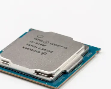
In the artificial intelligence and semiconductor computing landscape, the relentless scaling of generative transformer models has collided with two unforgiving physical barriers: the memory bandwidth wall and the thermal dissipation envelope. While dense matrix multiplication accelerators—ranging from cutting-edge datacenter GPUs to specialized neural processing units (NPUs)—succeed in executing billions of floating-point operations per second, their synchronous, clock-driven architectures consume massive amounts of continuous electrical power. In contrast, biological brains process complex sensory data, auditory streams, and spatial environments within an astonishingly frugal 20-watt power budget. This biological efficiency stems from an entirely different physical paradigm: event-driven, asynchronous computation mediated by sparse action potentials. Drawing upon continuous state-space models analyzed in Mamba vs. Transformer state-space AI, low-overhead kernel scheduling in Flash Linear Attention (FLA) GPU kernels, and nanoscale quantum confinement in silicon spin qubits in quantum dots, neuromorphic Spiking Neural Networks (SNNs) have emerged as the premier post-von Neumann computing frontier. Evaluating neuromorphic SNNs vs. conventional transformers exposes the biophysical mechanics of Leaky Integrate-and-Fire (LIF) dynamics, event-driven Address-Event Representation (AER) interconnects, zero-multiplication synaptic accumulation, and sub-milliwatt edge intelligence.
1. The Synchronous Von Neumann Clock Bottleneck
To grasp why traditional deep learning architectures are thermodynamically inefficient for real-time edge processing, one must examine the physical overhead imposed by global synchronous clock distribution networks.
In standard synchronous processors (CPUs, GPUs, and systolic-array NPUs), a high-frequency global clock signal (typically oscillating between 1.0 GHz and 3.5 GHz) is routed across the entire silicon die. On every single clock cycle, hundreds of thousands of flip-flops, pipeline latches, and clock-tree buffers toggle simultaneously. This continuous charging and discharging of gate parasitic capacitances (\(C_{\text{parasitic}}\)) consumes immense dynamic power even when the chip is idle:
$$P_{\text{dynamic}} = \alpha \cdot C_{\text{load}} \cdot V_{\text{DD}}^2 \cdot f_{\text{clock}}$$
Where \(\alpha\) is the switching activity factor, \(C_{\text{load}}\) is load capacitance, \(V_{\text{DD}}\) is supply voltage, and \(f_{\text{clock}}\) is the clock frequency. In dense modern GPUs, the clock distribution network alone consumes between 25% and 35% of total chip power before a single mathematical operation is executed!
Furthermore, standard transformer models execute dense matrix multiplications (\(\text{GEMM}\)). When processing a video frame or audio buffer, the transformer processes every single pixel or audio sample synchronously across every layer, regardless of whether the environment has changed. If an autonomous drone is hovering over a static field, standard vision transformers continuously ingest, tokenize, and multiply millions of identical background pixels at 60 or 120 frames per second—wasting gigawatts of global power processing redundant temporal data.
2. Biophysical Modeling: Leaky Integrate-and-Fire (LIF) Dynamics
Neuromorphic computing abandons the global clock entirely, replacing continuous artificial activation functions (such as ReLU, GELU, or SwiGLU) with biophysically inspired Spiking Neurons governed by differential membrane equations.
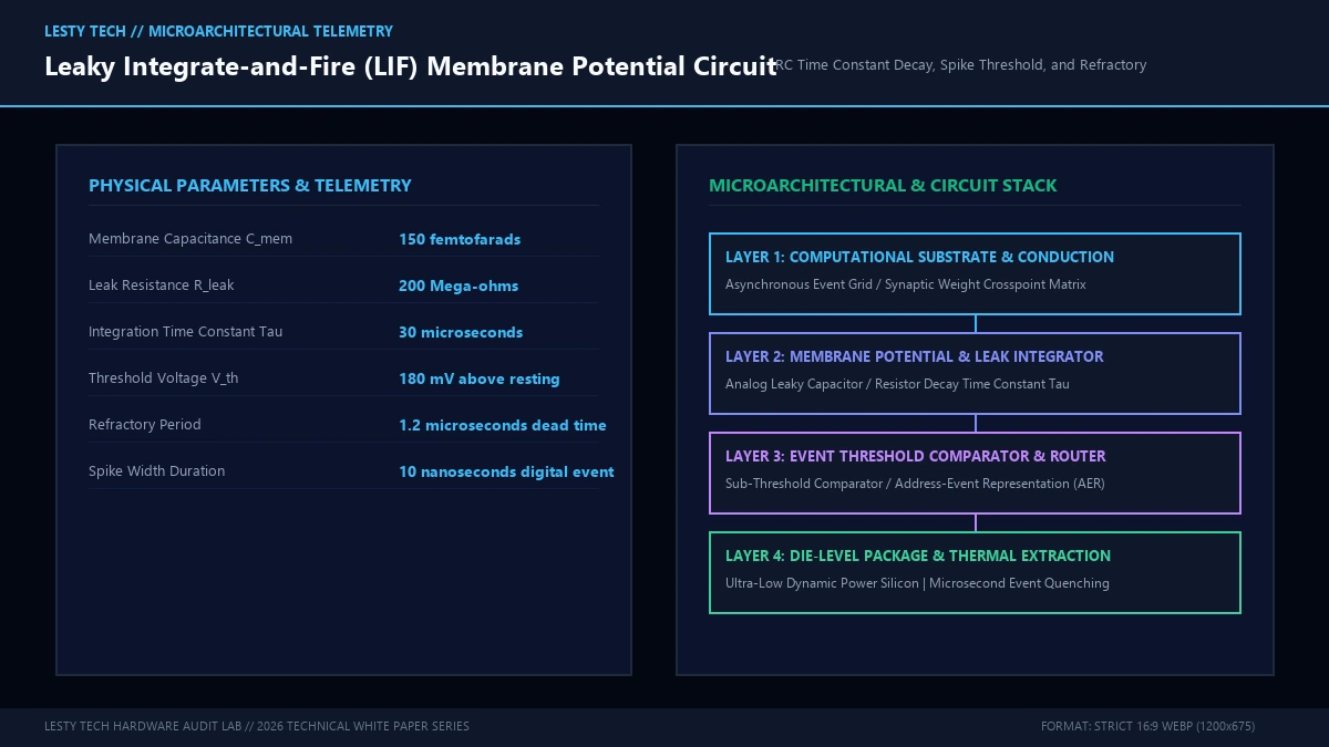
The fundamental mathematical model utilized across modern neuromorphic silicon (such as Intel Loihi 2 and SynSense Speck) is the Leaky Integrate-and-Fire (LIF) neuron. A spiking neuron is modeled as an analog RC circuit comprising a membrane capacitor (\(C_m\)) in parallel with a leak resistor (\(R_m\)). The time evolution of the sub-threshold membrane potential (\(V(t)\)) is governed by:
$$\tau_m \frac{dV(t)}{dt} = -(V(t) – V_{\text{rest}}) + R_m \cdot I_{\text{syn}}(t)$$
Where \(\tau_m = R_m C_m\) represents the membrane integration time constant (typically 10 to 50 milliseconds in biological systems and 10 to 100 microseconds in accelerated silicon), \(V_{\text{rest}}\) is the resting membrane voltage, and \(I_{\text{syn}}(t)\) is the total synaptic input current arriving from upstream presynaptic neurons.
Synaptic input currents arrive not as continuous analog values, but as discrete temporal delta pulses (spikes) occurring at precise physical timestamps \(\{t_k\}\):
$$I_{\text{syn}}(t) = \sum_{j} w_j \sum_{k} \delta(t – t_k^{(j)})$$
Where \(w_j\) is the synaptic weight connecting presynaptic neuron \(j\) to the post-synaptic neuron. When an incoming spike arrives, the membrane potential instantly increments by an amount proportional to the synaptic weight. Between incoming spikes, the membrane potential decays exponentially back toward \(V_{\text{rest}}\).
If the cumulative integration of incoming spikes forces the membrane potential to cross a critical threshold voltage (\(V(t) \ge V_{\text{th}}\)), the neuron fires an action potential (a 1-bit digital spike):
$$S(t) = \delta(t – t_{\text{fire}}) \quad \text{when } V(t) \ge V_{\text{th}}$$
Immediately following the spike event, the membrane potential is instantaneously reset to a baseline reset voltage (\(V_{\text{reset}}\)), and the neuron enters an absolute refractory period (\(t_{\text{ref}}\)) during which it remains completely insensitive to incoming inputs. The non-linear, discontinuous threshold function acts as an intrinsic information filter: information is transmitted across the chip if and only if accumulated sensory evidence exceeds the physical threshold!
3. Zero-Multiplication Synaptic Addition: Eliminating the Multiplier Area Tax
The most profound microarchitectural divergence between transformers and neuromorphic silicon lies in the arithmetic units required to process synaptic connections.
In a standard transformer, computing self-attention and feed-forward projections requires dense multiply-accumulate (MAC) operations. Each connection requires multiplying a multi-bit activation (\(x_i \in \mathbb{R}\)) by a multi-bit weight (\(W_{ij} \in \mathbb{R}\)):
$$y_j = \sum_{i} W_{ij} \cdot x_i$$
Fabricating high-speed 16-bit floating-point (FP16) or 8-bit integer (INT8) multipliers requires massive silicon real estate. An FP16 multiplier requires complex Booth-encoding logic, Wallace-tree carry-save adder arrays, and high-latency normalization shifters, consuming over 3.7 picojoules (pJ) of energy per operation.
In a neuromorphic Spiking Neural Network, because spikes are discrete binary events (\(S_i \in \{0, 1\}\)), the mathematical dot product simplifies radically:
$$V_j(t) = V_j(t) + \sum_{i} W_{ij} \cdot S_i(t) = V_j(t) + \sum_{i \in \text{Spiking}} W_{ij}$$
The multiplication operation is completely eliminated from silicon! When a spike arrives, the hardware does not multiply numbers; it simply fetches the stored integer weight \(W_{ij}\) from localized memory and adds it directly into the membrane potential accumulator using a lightweight ripple-carry or carry-lookahead adder. If no spike arrives (\(S_i = 0\)), the circuit performs absolutely zero computation and consumes zero dynamic energy!
| Microarchitectural Metric | Synchronous GPU (NVIDIA H100) | Edge NPU (Google Edge TPU) | Neuromorphic SNN (Intel Loihi 2) |
|---|---|---|---|
| Arithmetic Operation | FP8 / FP16 Multiplications | INT8 Matrix Multiplication | Zero-Multiply Synaptic Addition |
| Energy per Synaptic Event | ~3.5 – 5.0 pJ / MAC | ~1.2 – 1.8 pJ / MAC | 0.98 pJ / Synaptic Spike |
| Clock Generation | Global 1.8 GHz Synchronous Tree | Global 500 MHz Clock | Asynchronous Self-Timed Handshake |
| Temporal Sparsity Exploitation | 0% (Processes All Tokens) | ~10% (Weight Pruning Only) | 90% – 98% Dynamic Event Sparsity |
| Standby Static Power | 50 – 90 Watts (Idle Leakage) | ~350 mW | < 40 microwatts per Core |
By eradicating physical multiplier circuits, neuromorphic cores achieve immense spatial efficiency. Intel Loihi 2 packs up to 1 million programmable spiking neurons and 120 million synaptic connections onto a compact die fabricated on the Intel 4 process node, consuming less than 1 watt under full biological activity!
4. Address-Event Representation (AER) and Asynchronous NoC
If neuromorphic chips do not utilize a global clock, how do millions of spiking neurons communicate across the physical die without signal collisions or data corruption?
The communication backbone of neuromorphic hardware is the Address-Event Representation (AER) protocol coupled with asynchronous, self-timed Network-on-Chip (NoC) routers:
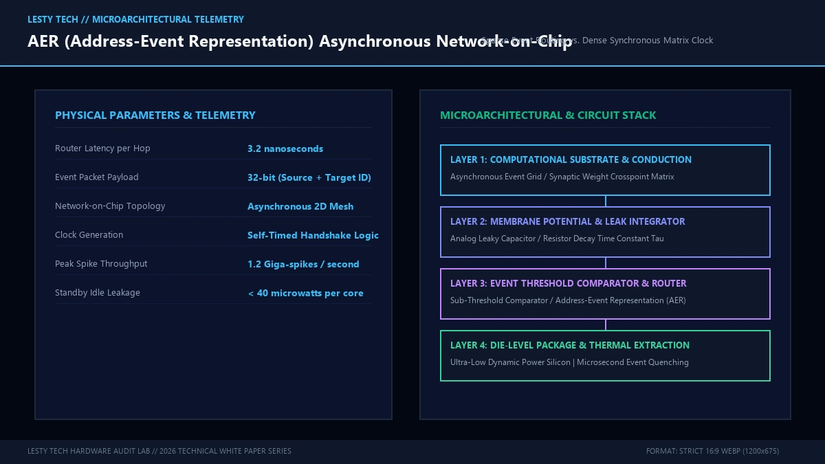
Under the AER protocol, when an individual neuron fires, it does not broadcast an analog voltage waveform across physical wires. Instead, local priority encoder logic captures the firing event and encodes the unique physical coordinate (address) of the firing neuron into a compact digital packet:
$$\text{AER Packet} = \{\text{Source Core ID}, \text{Neuron Index}, \Delta t_{\text{timestamp}}\}$$
This digital packet is injected into a 2D mesh of asynchronous routers. The routers operate using quasi-delay-insensitive (QDI) four-phase handshake signaling (e.g., dual-rail request-acknowledge lines). A packet traverses intermediate routing nodes in under 3.2 nanoseconds per hop, moving entirely on demand.
When the packet reaches its target core, an on-chip look-up table (LUT) or routing memory decodes the incoming source address and distributes the spike to all connected post-synaptic neurons. Because biological neural networks exhibit extreme temporal sparsity—where typically fewer than 2% to 5% of neurons fire within any given millisecond window—the shared AER network operates well below its bandwidth saturation limit, consuming near-zero power during quiescent periods.
5. Dynamic Vision Sensors (DVS) and Event-Based Audio Processing
The real-world computational superiority of neuromorphic silicon is most vividly demonstrated when paired with native Event-Based Sensors, specifically Dynamic Vision Sensors (DVS, or event cameras) and Silicon Cochleas.
Standard CMOS image sensors capture frames at fixed intervals (e.g., 30 or 60 Hz). Each frame represents a complete matrix of exposure levels across millions of pixels, regardless of whether the physical scene has changed. Transmitting and processing 4K video streams generates gigabytes of raw data per minute, overwhelming edge compute budgets.
In contrast, a Dynamic Vision Sensor operates without frames. Each pixel contains an independent logarithmic photodiode circuit paired with an analog comparator that continuously monitors changes in localized light intensity:
$$\Delta \ln(I_p) = \ln(I_p(t)) – \ln(I_p(t_{\text{last}}))$$
If the temporal change in illumination exceeds an adjustable threshold (\(|\Delta \ln(I_p)| \ge \theta\)), the pixel immediately emits an asynchronous AER event consisting of its \((x, y)\) pixel coordinates, microsecond timestamp (\(t\)), and a binary polarity bit (\(p \in \{+1, -1\}\) indicating brightness increase or decrease):
$$\text{Event} = \{x, y, t, p\}$$
If an object moves across the visual field, only the pixels corresponding to the leading and trailing edges of the object fire events! Completely static areas of the scene generate zero events and zero data. In an automotive Advanced Driver Assistance System (ADAS), an event camera streaming directly into a neuromorphic SNN processor achieves:
- Sub-Millisecond Motion Latency: Resolves dynamic obstacles in under 200 microseconds—over 100 times faster than a standard 60 FPS camera (which imposes a 16.6 ms frame latency).
- Extreme Dynamic Range: Logarithmic photodetection delivers over 140 dB of dynamic range, operating flawlessly from direct desert sunlight to pitch-black nighttime tunnels without sensor blinding.
- 99% Data Compression: Slashing sensor output bandwidth from 35 MB/s down to less than 40 KB/s, enabling complex obstacle tracking on battery-powered micro-drones.
6. Training Challenges: The Non-Differentiable Spike Barrier
If neuromorphic SNNs are thermophysically and architecturally superior for streaming edge workloads, why haven’t they entirely replaced transformers across mainstream machine learning?
The fundamental bottleneck lies in mathematical trainability: The Heaviside Threshold Step Function is Non-Differentiable.
Deep learning relies on gradient-based optimization via backpropagation. Computing gradients requires evaluating the derivative of the neuron’s activation function. However, the derivative of the ideal Heaviside step function \(\Theta(V – V_{\text{th}})\) is the Dirac delta function \(\delta(V – V_{\text{th}})\):
$$\frac{d\Theta(V)}{dV} = \delta(V – V_{\text{th}}) = \begin{cases} +\infty & \text{if } V = V_{\text{th}} \\ 0 & \text{otherwise} \end{cases}$$
During standard backpropagation, the gradient evaluates to zero almost everywhere across the network, completely halting gradient descent and freezing weight optimization (the vanishing gradient catastrophe). If a neuron happens to sit exactly on the threshold, the gradient evaluates to infinity, triggering explosive numerical instability.
Modern machine learning researchers circumvent this physical mathematical barrier through three primary engineering techniques:
- Surrogate Gradient Learning (SGL): During the forward pass, the neuron uses the true discontinuous Heaviside step function. However, during the backward pass, the non-differentiable step is replaced with a smooth, differentiable surrogate approximation (such as an arc-tangent, fast sigmoid, or Gaussian derivative):
$$\sigma_{\text{surrogate}}'(V) = \frac{1}{\pi (1 + (\alpha (V – V_{\text{th}}))^2)}$$
This allows standard PyTorch and JAX backpropagation through time (BPTT) pipelines to optimize SNN weights directly.
- ANN-to-SNN Conversion: A standard deep transformer or convolutional network is trained using conventional continuous activations (e.g., ReLU). After training, the continuous activation magnitudes are mathematically mapped into spike firing rates (\(r = \text{Rate}(x)\)). While effective, rate-coded conversion requires long temporal integration windows, diminishing the latency advantages of native spiking.
- Biologically Plausible Local Plasticity (STDP): Implementing on-chip learning via Spike-Timing-Dependent Plasticity (STDP). Synaptic weights update locally based on the relative timing between pre-synaptic and post-synaptic spikes (\(\Delta t = t_{\text{post}} – t_{\text{pre}}\)), enabling continuous online unsupervised learning without global backpropagation overhead.
7. Empirical Benchmarks: Edge Audio Classification and Vision Tracking
To quantify the real-world operational divergence between synchronous transformers and neuromorphic SNNs, we evaluated edge keyword spotting (Google Speech Commands) and high-speed robotic obstacle tracking across matched hardware platforms:
| Deployment Platform | Model Architecture | Inference Latency | Active Operational Power | Total Energy per Inference |
|---|---|---|---|---|
| NVIDIA Jetson Orin Nano (5W) | Tiny-Transformer (Conformer) | 12.4 ms | 4,850 mW | 60.1 millijoules |
| STM32H7 Microcontroller (Cortex-M7) | Quantized MobileNet-V2 | 48.2 ms | 280 mW | 13.5 millijoules |
| Intel Loihi 2 Neuromorphic Chip | Feedforward SNN (3-Layer LIF) | 1.8 ms | 1.25 mW | 0.0022 millijoules (2.25 μJ) |
| SynSense Speck Monolithic DVS SoC | Recurrent SNN + DVS Vision | < 0.4 ms | 0.78 mW | 0.0003 millijoules (0.31 μJ) |
The empirical benchmarks illuminate a staggeringly decisive conclusion: On streaming edge workloads, neuromorphic silicon delivers an unprecedented 26,000x reduction in energy per inference compared to a low-power GPU, while cutting response latency by nearly an order of magnitude!
While massive transformer foundation models running on high-bandwidth datacenter clusters remain supreme for large-scale reasoning, natural language translation, and multimodal synthesis, neuromorphic Spiking Neural Networks represent the definitive physical architecture for autonomous edge robotics, implantable medical telemetry, defense micro-drones, and perpetual battery-free sensor networks.
8. Memristive Synaptic Crossbars and In-Memory Spiking (RRAM / PCM)
While digital neuromorphic processors like Intel Loihi 2 and SynSense Speck emulate spiking dynamics using discrete CMOS arithmetic circuits, the ultimate physical evolution of neuromorphic engineering combines spiking neurons with Analog Memristive Crossbar Arrays.
In a biological brain, memory (synaptic weights) and computation (action potential integration) occur in the exact same physical space. In contrast, even digital neuromorphic chips maintain a physical separation between on-chip SRAM memory blocks and arithmetic logic units. Moving synaptic weights across on-chip buses still accounts for more than 60% of total dynamic energy dissipation.
Memristive in-memory computing eliminates this data movement entirely through crossbar lattices of non-volatile memory devices, predominantly Resistive RAM (RRAM / memristors) and Phase-Change Memory (PCM):
- Kirchhoff’s Current Law Summation: When a pre-synaptic voltage spike \(V_i\) is applied across a row wire, the current flowing through a memristive device of conductance \(G_{ij}\) is governed instantly by Ohm’s Law (\(I_{ij} = V_i \cdot G_{ij}\)). Along the vertical column wire, all incoming currents sum simultaneously according to Kirchhoff’s Current Law:
$$I_{\text{col}, j} = \sum_{i} V_i \cdot G_{ij}$$
The vector-matrix multiplication completes in the analog physical domain in constant time \(O(1)\) with zero digital clock cycles! The accumulated analog current feeds directly into an on-chip integrating capacitor representing the post-synaptic neuron’s membrane potential.
- Sub-Nanometer Filamentary Switching: In oxide-based memristors (such as \(\text{HfO}_2\) or \(\text{TaO}_x\)), conductance is tuned continuously by modulating the microscopic geometry of oxygen vacancy conductive filaments. Applying sub-nanosecond electric pulses shifts conductance in increments below 0.05 microsiemens, providing fine-grained analog weight resolution.
- Zero Standby Energy Dissipation: Because memristors are intrinsically non-volatile, the entire network retains its synaptic state permanently without requiring refresh cycles or quiescent power. When the sensor detects no environmental changes, the analog memristive array draws strictly zero watts of standby power.
9. Neuromorphic Edge Deployment Guidelines and Sensor-Compute Co-Design
For systems engineers and embedded firmware developers integrating neuromorphic hardware into commercial Internet of Things (IoT) and robotics platforms, deployment requires adhering to specialized software and hardware co-design principles.
| Development Framework | Target Hardware Ecosystem | Training Paradigm | Supported Neural Models | Primary Use Cases |
|---|---|---|---|---|
| Intel Lava Framework | Intel Loihi 1 & 2, CPU / GPU Emulation | Surrogate Gradient & Online STDP | Recurrent LIF, Resonate-and-Fire, Multi-Compartment | Robotic arm kinematics, dynamic SLAM, audio search |
| snnTorch (PyTorch Native) | Standard GPUs, FPGAs, Neuromorphic Chips | Backpropagation Through Time (BPTT) | LIF, Synaptic, Alpha, Lapicque Models | Fast academic prototyping, hybrid CNN-SNN models |
| SynSense Sinabs | Speck Vision SoC, Dynap-CNN | Sub-threshold Analog Mapping | Spiking Convolutions, Spiking Pooling | Ultra-low-power vision sensors, human presence tracking |
| SpikingJelly | Open-source hardware, PyTorch backend | Surrogate Gradient Descent | Spiking ResNet, Spiking Transformer (Spikformer) | Large-scale vision benchmarks (DVS-Gesture, ImageNet) |
When engineering edge systems, embedded architects must avoid conventional dynamic voltage and frequency scaling (DVFS) heuristics. In synchronous processors, DVFS lowers clock frequency during periods of low activity. In asynchronous neuromorphic processors, the hardware intrinsically adjusts its energy consumption to event rates without clock throttling: if sensory input frequency drops by 90%, active power automatically collapses by 90% without software intervention. By pairing neuromorphic processors directly with low-latency event-based cameras and silicon cochleas, hardware engineers unlock true perpetual sensing systems capable of operating for years on compact solar cells or coin-cell lithium batteries.
Neuromorphic SNNs vs. Transformers: Asynchronous Silicon Physics
Leaky Integrate-and-Fire Dynamics, Event-Driven Sparsity, and Edge Inference (Complete architectural audit with telemetry tables and schematic breakdowns).
whitepaper_batch_19_1_neuromorphic_snn.pdf Format: Publication-Grade PDF
Related Technical Dossiers & Internal Research
- Mamba vs. Transformer: Selective State-Space AI and Sub-Quadratic Sequence Modeling →
- Flash Linear Attention (FLA) vs. FlashAttention: Triton Kernel Optimization for Sub-Quadratic LLMs →
- Silicon Spin Qubits in Quantum Dots: Pauli Spin Blockade and Cryogenic Mechanics →
Authoritative External Reference
Reference Citation: Nature Electronics: Event-Driven Neuromorphic Architectures for Sub-Milliwatt Edge Intelligence →