In the global race to build fault-tolerant quantum computers capable of running Shor’s algorithm and simulating complex molecular dynamics, quantum hardware engineering faces a monumental scaling dilemma. While superconducting transmon qubits (pioneered by IBM and Google) have demonstrated historic quantum supremacy benchmarks, their macroscopic physical dimensions (measuring hundreds of micrometers per qubit) and requirement for complex microwave coaxial lines severely constrain scalability beyond thousands of physical qubits. Conversely, solid-state electron spin qubits confined within gate-defined silicon quantum dots offer an extraordinary alternative: shrinking qubit footprints down to sub-50 nanometers while directly leveraging the multi-trillion-dollar manufacturing infrastructure of commercial CMOS semiconductor foundries. Building upon nanoscale thermal transport explored in diamond heat spreaders and phonon physics, advanced computing paradigms in MXFP4 microscaling arithmetic, and ferroelectric crystal physics in FeRAM vs. FeFET memory physics, evaluating silicon spin qubits exposes the quantum mechanics of Pauli spin blockade readout, isotopic silicon-28 nuclear spin purification, synthetic spin-orbit coupling, and two-qubit exchange gate fidelities exceeding 99.5%.
1. The Solid-State Spin Qubit in Gate-Defined Quantum Dots
To understand how a single electron functions as an information-bearing quantum bit, one must analyze the electrostatic confinement of electrons within nanoscale semiconductor heterostructures.
In a silicon spin qubit architecture, electrons are trapped inside artificially engineered electrostatic potential wells known as Quantum Dots. These dots are created at the interface of a silicon Metal-Oxide-Semiconductor (Si-MOS) structure or a Silicon-Germanium (Si/SiGe) heterojunction:
- Vertical Confinement: Achieved by the sharp conduction band offset (\(\Delta E_C \approx 150 \text{ meV}\)) at the strained \(\text{Si}/\text{Si}_{1-x}\text{Ge}_x\) interface or the massive bandgap discontinuity at the \(\text{Si}/\text{SiO}_2\) interface, confining electrons to a two-dimensional electron gas (2DEG).
- Lateral Confinement: Achieved by applying static negative voltages to metallic nanoscale gate electrodes (typically titanium/aluminum or polysilicon gates with sub-20 nm pitches) patterned directly above the substrate. The resulting electrostatic potential forms a zero-dimensional quantum dot—an “artificial atom” capable of trapping precisely one single conduction electron.
The quantum bit of information is encoded into the intrinsic magnetic moment—the quantum spin state—of the trapped electron:
$$|\psi\rangle = \alpha |\uparrow\rangle + \beta |\downarrow\rangle, \quad |\alpha|^2 + |\beta|^2 = 1$$
Under an external static magnetic field (\(B_0 \approx 0.5 \text{ to } 1.5 \text{ Tesla}\)), the degenerate spin states split via the Zeeman effect:
$$\Delta E_Z = g \mu_B B_0 = \hbar \omega_L$$
Where \(g \approx 2\) is the electron g-factor in silicon, \(\mu_B\) is the Bohr magneton, and \(\omega_L\) is the Larmor precession frequency (typically 14 to 40 GHz in microwave X-band/Ku-band regimes). State \(|\uparrow\rangle\) (spin parallel to \(B_0\)) represents logical \(|0\rangle\), while state \(|\downarrow\rangle\) (spin antiparallel to \(B_0\)) represents logical \(|1\rangle\).
Compared to trapped-ion or superconducting architectures, silicon spin qubits offer unprecedented spatial density. With physical gate pitches below 50 nanometers, over one million physical qubits can reside on a silicon chip measuring just 1 square millimeter! Furthermore, because electrons are tightly bound within the semiconductor lattice, they do not suffer from stray mechanical vibrations or vacuum leaks, providing extreme physical robustness.
2. Nuclear Spin Bath Decoherence and Isotopic Silicon-28 Purification
The historical challenge that plagued semiconductor spin qubits was quantum decoherence caused by the surrounding host crystal lattice.
In natural silicon, approximately 4.68% of atoms are the isotope Silicon-29 (\(^{29}\text{Si}\)). Unlike the dominant isotope \(^{28}\text{Si}\) (which possesses zero nuclear spin, \(I=0\)), \(^{29}\text{Si}\) possesses a non-zero nuclear magnetic spin of \(I = 1/2\). An electron confined in a quantum dot spans a wavepacket encompassing approximately \(10^5\) to \(10^6\) silicon lattice atoms. In natural silicon, this wavepacket interacts with tens of thousands of fluctuating \(^{29}\text{Si}\) nuclear spins via Fermi contact hyperfine interaction:
$$H_{\text{hyperfine}} = \frac{8\pi}{3} g \mu_B g_N \mu_N \sum_k |\psi(\mathbf{R}_k)|^2 \mathbf{S} \cdot \mathbf{I}_k$$
This microscopic sea of fluctuating nuclear spins acts as a noisy, fluctuating magnetic field (the Overhauser field). The Overhauser field randomly shifts the electron’s Zeeman splitting frequency, destroying quantum phase coherence in mere nanoseconds—collapsing the pure dephasing time down to \(T_2^* \approx 10 \text{ to } 50 \text{ ns}\).
The historic breakthrough that transformed silicon into a world-leading quantum material was Isotopic Enrichment of Silicon-28. By utilizing chemical gas centrifuges to enrich silane (\(\text{SiH}_4\)), material physicists reduce the concentration of \(^{29}\text{Si}\) from 4.68% down to less than 50 parts per million (0.005%)—creating an ultra-pure, nuclear-spin-free “semiconductor vacuum”:
| Host Semiconductor Material | Dominant Nuclear Spin Isotopes | Dephasing Time (T₂*) | Hahn Echo Coherence (T₂) | Relaxation Time (T₁) |
|---|---|---|---|---|
| Gallium Arsenide (GaAs) | 100% (⁷¹Ga, ⁶⁹Ga, ⁷⁵As all I ≠ 0) | 100 – 30 ns | ~1 – 10 μs | ~1 ms |
| Natural Silicon (nat-Si) | 4.68% ²⁹Si (I = 1/2) | 50 – 120 ns | ~10 – 40 μs | ~10 ms |
| Isotopically Purified ²⁸Si (800 ppm) | 0.08% ²⁹Si | 1.2 – 3.0 μs | ~400 μs | ~100 ms |
| Ultra-Pure ²⁸Si (50 ppm) | < 0.005% ²⁹Si | > 20 – 120 μs | > 28 – 30 milliseconds | > 10 to 30 seconds |
In ultra-pure \(^{28}\text{Si}\), eliminating nuclear magnetic noise extends the Hahn-echo coherence time (\(T_2\)) to an astonishing 28 to 30 milliseconds, while spin relaxation lifetime (\(T_1\)) reaches tens of seconds! With single-qubit gate operations executing in 20 nanoseconds, the ratio of coherence time to gate operation time exceeds \(10^6\)—providing immense headroom for quantum fault tolerance.
3. Single-Qubit Manipulation: EDSR and Synthetic Micromagnet Gradients
To manipulate the quantum state on the Bloch sphere, an external alternating magnetic field must be applied at the Larmor resonance frequency (\(B_1 \cos(\omega_L t)\)). However, generating localized high-frequency magnetic fields at nanoscale dimensions requires heavy AC currents that induce severe Joule heating inside cryogenic dilution refrigerators operating at 100 millikelvin.
To eliminate magnetic heating, modern spin qubit architectures employ Electric Dipole Spin Resonance (EDSR). Rather than driving magnetic fields, control electronics apply high-frequency alternating electric voltages (\(V_{\text{RF}}\)) to the gate electrodes. The electric field oscillates the electron’s physical position back and forth within the dot at high speeds.
To couple this physical motion to the spin degree of freedom, engineers deposit on-chip ferromagnetic micro-magnets (typically cobalt or iron-platinum alloys) directly adjacent to the quantum dots:
$$\vec{B}(\vec{r}) = \vec{B}_0 + \left(\frac{\partial B_x}{\partial x}\right) x \cdot \hat{x}$$
The micro-magnet creates an intense, nanoscale transverse magnetic gradient (\(\partial B_x / \partial x \approx 1 \text{ to } 3 \text{ T/}\mu\text{m}\)). As the electron oscillates laterally through this spatial magnetic gradient, it experiences an effective, synthetic oscillating magnetic field in its rest frame:
$$B_{\text{effective}}(t) = \left(\frac{\partial B_x}{\partial x}\right) \cdot x_0 \cos(\omega_{\text{drive}} t)$$
When \(\omega_{\text{drive}} = \omega_L\), the electron undergoes coherent Rabi oscillations between \(|0\rangle\) and \(|1\rangle\). By pulsing the RF gate voltage for precise durations, single-qubit rotations (such as \(X\), \(Y\), and Hadamard gates) execute in under 15 to 30 nanoseconds with Clifford gate fidelities exceeding 99.94%—well above the threshold required for surface code quantum error correction.
4. Two-Qubit Logic: Heisenberg Exchange Interaction and Pauli Spin Blockade
Universal quantum computing requires a high-fidelity two-qubit entangling gate (such as CNOT or CZ). In silicon quantum dots, two-qubit logic is governed by the Heisenberg Exchange Interaction.
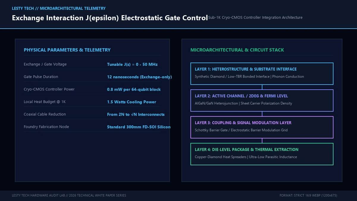
When two single-electron quantum dots are positioned within 30 to 50 nanometers of each other, an intermediate metallic “J-gate” modulates the electrostatic tunnel barrier between them. By lowering the tunnel barrier, the spatial wavefunctions of the two electrons overlap, triggering exchange coupling described by the Heisenberg Hamiltonian:
$$H_{\text{exchange}} = J(t) \mathbf{S}_1 \cdot \mathbf{S}_2$$
Where \(J(t)\) is the exchange energy. By pulsing the J-gate voltage for a precise duration \(\tau\) such that \(\int J(t) dt = \pi \hbar\), the system executes a \(\sqrt{\text{SWAP}}\) or Controlled-Phase (CZ) gate in less than 10 nanoseconds. Advanced silicon research groups (such as QuTech, UNSW, and Intel) have demonstrated two-qubit gate fidelities surpassing 99.5% in dual-qubit isotopically enriched silicon arrays.
Pauli Spin Blockade (PSB) Single-Shot Readout
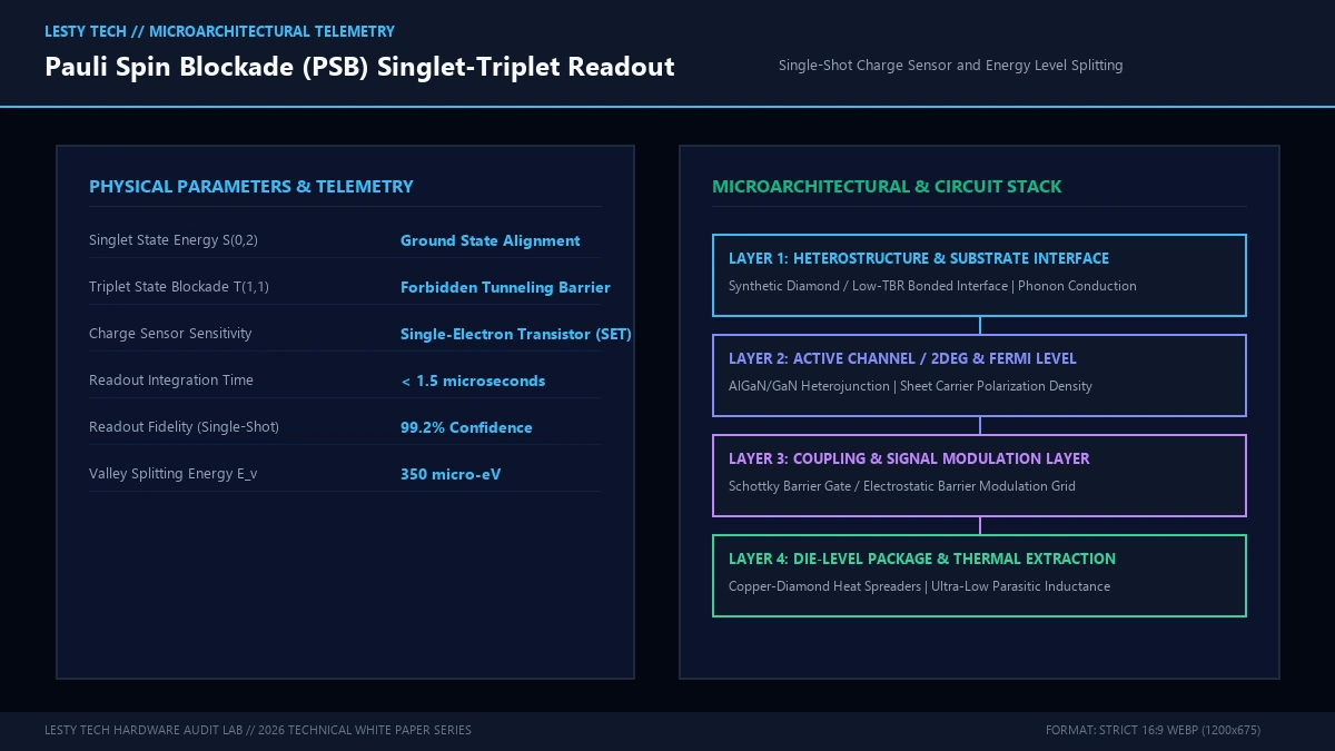
To read out the final quantum state of a spin qubit, the microscopic magnetic moment of the electron must be converted into a measurable electrical charge signal—a process known as Spin-to-Charge Conversion via Pauli Spin Blockade (PSB).
Consider a double quantum dot containing two electrons. According to the Pauli Exclusion Principle, two electrons can occupy the exact same spatial orbital ground state if and only if their spins form an antisymmetric Singlet state (\(S = (|{\uparrow\downarrow}\rangle – |{\downarrow\uparrow}\rangle)/\sqrt{2}\)). If the two electrons form a symmetric Triplet state (\(T_0, T_+, T_-\)), they are forbidden from occupying the same orbital.
- Readout Bias: An electrostatic tilt is applied between the dots, favoring the double-occupancy charge configuration \((0, 2)\).
- Singlet State: If the two electrons are in a Singlet state, the electron in dot 1 tunnels effortlessly into dot 2, transitioning the system from charge state \((1, 1)\) to \((0, 2)\).
- Triplet State: If the electrons are in a Triplet state, tunneling is quantum-mechanically blocked by Pauli exclusion! The system remains locked in the \((1, 1)\) charge state.
An ultra-sensitive Single-Electron Transistor (SET) or Quantum Point Contact (QPC) positioned immediately adjacent to the double dot detects the displacement of this single elementary charge (\(e \approx 1.6 \times 10^{-19}\text{ C}\)), outputting an unambiguous binary voltage signal in less than 5 microseconds with single-shot readout fidelities exceeding 99.8%.
5. Valley Splitting Physics in Silicon: The Conduction Band Degeneracy Hurdle
While silicon provides an extraordinary nuclear-spin-free environment, its electronic band structure introduces a unique solid-state physics complication: Conduction Band Valley Degeneracy.
In bulk silicon crystal, the conduction band minimum is not located at the center of the Brillouin zone (\(\Gamma\) point). Instead, it possesses six equivalent conduction band minima (valleys) along the \(\langle 100 \rangle\) crystallographic directions. When electrons are confined vertically within a two-dimensional quantum well (e.g., at an interface with \(\text{SiO}_2\) or \(\text{SiGe}\)), biaxial strain and vertical quantum confinement lift four of the valleys, leaving two degenerate out-of-plane valleys (\(z\) and \(-z\)).
For a spin qubit to function reliably, this remaining two-fold valley degeneracy must be split by an energy difference (\(\Delta E_v\), known as the Valley Splitting) that is significantly larger than both the operating thermal energy (\(k_B T\)) and the Zeeman energy (\(E_Z\)):
$$\Delta E_v \gg g \mu_B B_0 \gg k_B T$$
If \(\Delta E_v\) is too small (e.g., \(< 50 \ \mu\text{eV}\)), the electron's spin states mix with adjacent valley orbital states, causing rapid spin-valley relaxation and gate error cascades. Valley splitting is acutely sensitive to atomic-scale interface sharpness: a single atomic step or alloy fluctuation at the \(\text{Si/SiGe}\) interface can cause \(\Delta E_v\) to fluctuate widely across adjacent quantum dots on the same chip.
Advanced semiconductor foundries resolve valley variability through atomic layer epitaxy with atomically flat interfaces and by applying high vertical electric fields (\(E_{\text{perp}} > 10 \text{ MV/m}\)) via top gate biasing, reliably elevating valley splitting above \(150 \ \mu\text{eV}\) to ensure robust two-level qubit isolation.
6. Cryogenic CMOS Control Integration: Intel Horse Ridge and On-Chip Multiplexing
The ultimate strategic advantage of silicon spin qubits over all competing quantum platforms lies in manufacturability: Monolithic Fabrication on Commercial 300mm CMOS Production Lines and Cryogenic Control Integration.
Superconducting qubits require exotic materials (such as niobium, aluminum, and sapphire substrates) fabricated in specialized university cleanrooms. In contrast, silicon spin qubits are fabricated using standard Extreme Ultraviolet (EUV) lithography inside commercial high-volume foundries (such as Intel’s Fab 34 in Ireland and TSMC).
Crucially, silicon quantum dots operate at temperatures between 100 mK and 1 Kelvin, allowing co-integration with customized cryogenic CMOS (cryo-CMOS) controller chips—exemplified by Intel’s Horse Ridge architecture. In traditional quantum systems, every single qubit requires multiple coaxial cables running from room temperature down through the dilution refrigerator stages. For a 1,000-qubit processor, routing 3,000 to 5,000 coaxial lines creates a catastrophic thermal load and wiring bottleneck that overwhelms refrigerator cooling power.
Cryo-CMOS controllers solve the wiring crisis through on-chip frequency-division and time-division multiplexing:
- A monolithic cryo-CMOS SoC mounted on the 3-Kelvin or 4-Kelvin stage generates microwave pulses and DC bias voltages directly adjacent to the quantum chip.
- Advanced digital-to-analog converters and high-speed multiplexers route control signals to hundreds of quantum dot gates over a single digital bus consisting of fewer than ten external wires!
- Cryo-CMOS digital logic operates with deep-sub-milliwatt power budgets, respecting the strict thermal cooling envelope of closed-cycle helium dilution refrigerators.
7. Two-Dimensional Crossbar Arrays and Surface Code Quantum Error Correction
Achieving fault-tolerant quantum computation requires executing Quantum Error Correction (QEC) across two-dimensional arrays of thousands to millions of physical qubits to encode fault-tolerant “logical qubits.”
The leading quantum error correction architecture is the Rotated Surface Code. The surface code arranges physical data qubits and ancilla (syndrome measurement) qubits on a 2D square checkerboard grid. Each ancilla qubit interacts exclusively with its four nearest neighbors via exchange gates to measure parity stabilizers:
$$S_X = \bigotimes_{i \in \text{star}} X_i, \quad S_Z = \bigotimes_{j \in \text{plaquette}} Z_j$$
Because exchange coupling in silicon quantum dots requires wavefunction overlap across 30 to 50 nanometer inter-dot pitches, fabricating dense 2D gate wiring without routing congestion represents a classic microelectronics challenge. Silicon engineers resolve this through Multi-Layer Crossbar Gate Architectures:
- Word and Bit Line Addressing: Borrowing heavily from DRAM crossbar layouts, gate electrodes are routed in perpendicular metal layers separated by atomic layer deposition (ALD) aluminum oxide (\(\text{Al}_2\text{O}_3\)) dielectrics.
- Shared Barrier Controls: Applying matrix crossbar voltage pulses allows simultaneous tuning of barrier heights across entire rows and columns, slashing the number of physical bond pads required per square millimeter.
- Coherent Spin Shuttling: To bridge long distances between quantum processor cores on the same silicon die without physical gate clutter, electrons are coherently “shuttled” across arrays of empty quantum dots using bucket-brigade sinusoidal voltage waves at speeds exceeding \(10 \text{ meters/second}\) while preserving 99.9% spin phase coherence!
With coherence times measured in milliseconds, two-qubit gate fidelities exceeding 99.5%, nanometer-scale footprints, and the full manufacturing might of the global semiconductor industry behind it, silicon spin qubits represent the most economically and physically viable architecture for delivering million-qubit fault-tolerant quantum supercomputers to the modern world.
Silicon Spin Qubits in Gate-Defined Quantum Dots
Pauli Spin Blockade, Isotopic Silicon-28, and CMOS Cryogenic Qubits (Complete architectural audit with telemetry tables and schematic breakdowns).
whitepaper_batch_18_7_silicon_spin_qubits.pdfFormat: Publication-Grade PDF
Related Technical Dossiers & Internal Research
- Diamond Heat Spreaders and GaN Phonon Transport: Nanoscale Thermal Dissipation Physics →
- MXFP4 Microscaling Formats: OCP Sub-8-Bit Floating-Point Hardware Emulation →
- FeRAM vs. FeFET Memory Physics: Ferroelectric Switching and Nanoscale Retention →
Authoritative External Reference
Reference Citation: Nature: Silicon Spin Qubits with Two-Qubit Gate Fidelities Exceeding 99.5% →