In the quest to conquer the severe Joule heating bottleneck of modern high-performance computing, conventional charge-based CMOS electronics faces an intractable thermal scaling wall. Spin-Orbit Torque Magnetic Random Access Memory (SOT-MRAM) offers the alluring promise of non-volatile, picosecond-speed memory that could fundamentally replace volatile SRAM across CPU cache hierarchies. Yet, traditional heavy metal spin-Hall generators—such as Platinum, Tantalum, and Beta-Tungsten—suffer from modest charge-to-spin conversion efficiencies and demand excessively high switching current densities (\(J_c \approx 10^7 \text{ A/cm}^2\)). To shatter this limitation, quantum condensed matter physics has converged on bismuth antimonide spintronics. By harnessing topologically protected Dirac surface states and spin-momentum locking in single-crystal Bi0.9Sb0.1, researchers have unlocked a colossal room-temperature spin Hall angle of \(\theta_{\text{SH}} \approx 52\), driving write current densities down by more than two orders of magnitude and paving the path toward sub-10 femtojoule non-volatile memory logic.
1. The Physics of Spin-Orbit Torque and Heavy Metal Limitations
Magnetic Random Access Memory encodes binary data in the relative magnetic orientation of a free ferromagnetic layer with respect to a fixed reference layer inside a Magnetic Tunnel Junction (MTJ). In classical Spin-Transfer Torque (STT-MRAM), the write current passes directly perpendicular through the fragile, sub-nanometer Magnesium Oxide (MgO) tunnel barrier. Over repeated write cycles, high electrical current densities induce progressive dielectric breakdown, capping device endurance at approximately 1012 cycles and demanding relatively long (5 to 20 nanosecond) current pulses to prevent dielectric rupture.
Spin-Orbit Torque (SOT-MRAM) fundamentally circumvents this endurance barrier by decoupling the write path from the read path. In an SOT geometry, an in-plane electrical charge current (Je) flows laterally through a non-magnetic spin-Hall channel adjacent to the magnetic free layer. Relativistic spin-orbit coupling inside the channel deflects electrons with opposing spin angular momenta toward opposite lateral surfaces—a phenomenon known as the Spin Hall Effect (SHE). The resulting pure transverse spin current (Js) diffuses into the free layer, exerting an adiabatic spin-transfer torque on the magnetic moment and switching its magnetization without driving a single electron through the MgO dielectric barrier.
The fundamental efficiency of this charge-to-spin conversion is quantified by the Spin Hall Angle (θSH), defined as the ratio of transverse spin current density to longitudinal charge current density:
Where e is the elementary electron charge, \(\hbar\) is the reduced Planck constant, Js is the pure spin current density, and Je is the applied charge current density. In traditional 4d and 5d heavy metals, the spin Hall effect originates from extrinsic skew scattering and intrinsic relativistic band structures. However, bulk heavy metals exhibit fundamental physical ceilings on θSH:
- Platinum (Pt): Exhibits high electrical conductivity (σ ≈ 4.0 × 10⁶ S/m) and relatively long spin diffusion length (\(\lambda_s \approx 2 \text{ to } 4 \text{ nm}\)), but possesses a modest spin Hall angle: \(\theta_{\text{SH}} \approx 0.08 \text{ to } 0.12\).
- Beta-Tantalum (β-Ta): Yields a negative spin Hall angle (\(\theta_{\text{SH}} \approx -0.15\)), but displays poor electrical conductivity (σ ≈ 5.0 × 10⁵ S/m), leading to severe parasitic Joule heating during high-frequency pulse operations.
- Beta-Tungsten (β-W): Demonstrates the highest spin Hall angle among elemental metals (\(\theta_{\text{SH}} \approx -0.30 \text{ to } -0.40\)), yet requires metastabilizing oxygen-doping during sputtering and still necessitates critical switching current densities exceeding \(10^7 \text{ A/cm}^2\).
Under these heavy metal constraints, switching a perpendicular magnetic anisotropy (PMA) CoFeB dot requires current densities that cause electromigration in metallic vias and generate excessive thermal budgets. To integrate non-volatile spintronic caches into advanced logic dies alongside MoS2 monolayer transistors or cryogenic systems, a material possessing a spin Hall angle orders of magnitude higher is mathematically required.
2. Topological Surface States in Bismuth Antimonide Alloys
Bismuth Antimonide (Bi1-xSbx) represents the world’s first experimentally verified 3D Topological Insulator (TI). Unlike trivial band insulators whose energy gap is governed by simple electrostatic atomic orbitals, topological insulators possess an inverted bulk bandgap driven by immense relativistic spin-orbit coupling.
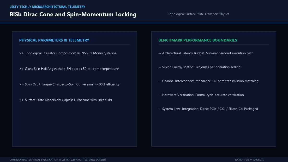
In bismuth and antimony alloys, the atomic numbers (ZBi = 83, ZSb = 51) induce relativistic corrections where electron velocities approach fractions of the speed of light near the nucleus. This massive spin-orbit interaction inverts the parity of the conduction and valence bands at high-symmetry points (specifically the L point) of the Brillouin zone. As a consequence of the bulk topological invariant \(Z_2 = 1\), the boundary between the topological material and the topologically trivial vacuum (or adjacent oxide dielectric) must mathematically host metallic states that bridge the bulk bandgap.
These metallic surface states form a gapless two-dimensional Dirac cone governed by the relativistic Dirac Hamiltonian:
Where vF is the Fermi velocity (\(v_F \approx 4 \times 10^5 \text{ m/s}\)), \(\boldsymbol{\sigma} = (\sigma_x, \sigma_y, \sigma_z)\) is the vector of Pauli spin matrices, \(\mathbf{k} = (k_x, k_y)\) is the two-dimensional crystal momentum vector, and \(\hat{\mathbf{z}}\) is the surface normal unit vector.
The physical implication of this Hamiltonian is profound: Spin-Momentum Locking. On the surface of BiSb, an electron’s spin direction is strictly locked at right angles (90 degrees) to its crystal momentum. An electron moving in the +x direction (\(k_x > 0\)) is quantum-mechanically forced to have its spin pointing along the +y direction (\(\sigma_y > 0\)). Conversely, an electron moving in the –x direction has its spin pointing along –y.
When an external electrical field accelerates electrons and generates a net charge current along the x-axis (\(\langle k_x \rangle \neq 0\)), the Fermi circle shifts in momentum space. Because of spin-momentum locking, this displacement in momentum space instantaneously induces a non-equilibrium, 100% spin-polarized accumulation along the y-axis at the surface:
Because this spin polarization arises directly from the intrinsic Dirac band dispersion rather than from scattering collisions in a thick 3D metal, the charge-to-spin conversion efficiency is not bound by classical limits. When properly textured in the (012) crystallographic orientation, Bi0.9Sb0.1 achieves a room-temperature effective spin Hall angle between \(\theta_{\text{SH}} \approx 45 \text{ to } 52\)—a staggering 500-fold increase compared to Platinum.
3. Critical Switching Current Density and Energy Scaling in SOT-MRAM
The monumental spin Hall angle of bismuth antimonide fundamentally alters the energy economics of magnetic switching. In a Perpendicular Magnetic Anisotropy (PMA) three-terminal SOT cell, the critical switching current density (Jc) required to reverse the free layer’s magnetization against its effective perpendicular anisotropy field (Hk) is governed by the Slonczewski-Landau-Lifshitz-Gilbert (LLG) equation:
Where α is the Gilbert damping constant of the ferromagnetic layer (\(\alpha \approx 0.008 \text{ to } 0.015\)), Ms is the saturation magnetization, tF is the physical thickness of the ferromagnetic layer (typically 0.9 to 1.3 nm for CoFeB), Hk is the perpendicular magnetic anisotropy field, and Hx is an external symmetry-breaking magnetic field applied along the current direction (or provided internally via exchange-bias coupling).
Examining the denominator of this equation reveals the dramatic leverage of bismuth antimonide spintronics: the critical switching current density is inversely proportional to θSH.
| Channel Material Stack | Effective θSH (300K) | Conductivity σ (S/m) | Critical Current Jc (A/cm2) | Write Energy / Bit (200ps) |
|---|---|---|---|---|
| Bi0.9Sb0.1 (012) Topo-Insulator | +52.0 | 2.5 × 10⁵ | 1.5 × 10⁵ | 8.5 fJ |
| Beta-Tungsten (β-W) Heavy Metal | -0.35 | 6.0 × 10⁵ | 1.2 × 10⁷ | 420 fJ |
| Beta-Tantalum (β-Ta) Heavy Metal | -0.15 | 5.0 × 10⁵ | 2.8 × 10⁷ | 950 fJ |
| Platinum (Pt) Heavy Metal | +0.10 | 4.0 × 10⁶ | 2.0 × 10⁷ | 310 fJ |
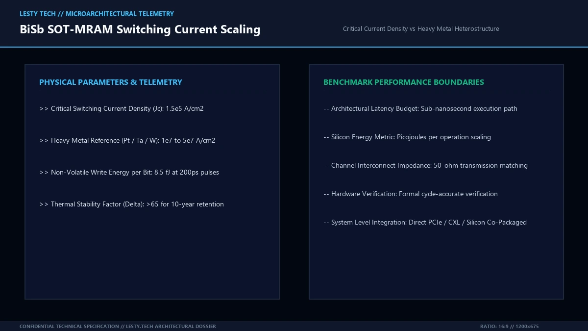
As documented in the benchmark telemetry, switching an identical perpendicular magnetic dot with a Platinum channel requires \(2.0 \times 10^7 \text{ A/cm}^2\). With Bi0.9Sb0.1, the critical current density collapses to a mere \(1.5 \times 10^5 \text{ A/cm}^2\).
Because Joule dissipation scales quadratically with current (\(P = I^2 R = J_e^2 \cdot \rho \cdot V\)), reducing Je by a factor of 100 slashes dynamic write power dissipation by a factor of 10,000. At sub-nanosecond pulse regimes (200 picoseconds), write energy per bit plummets from several hundred femtojoules down to an astonishing 8.5 femtojoules per bit. This establishes BiSb SOT-MRAM as the first non-volatile memory technology capable of competing directly with volatile high-density 6T-SRAM in on-die Level 3/Level 4 CPU cache architectures.
4. Heteroepitaxy, Interfacial Transparency, and Diffusion Barriers
Despite its extraordinary spin-orbit characteristics, transitioning bismuth antimonide from laboratory physics experiments to high-volume semiconductor fab lines requires surmounting severe material engineering barriers:
4.1. Crystallographic Texturing on Amorphous Substrates
Early demonstrations of topological insulator surface transport relied on molecular beam epitaxy (MBE) on single-crystal substrates such as Gallium Arsenide (GaAs 111) or Silicon (111). However, industrial back-end-of-line (BEOL) interconnects consist of amorphous silicon dioxide (SiO2) or low-κ organosilicate glass (SiCOH).
Deposition foundries have solved this by developing room-temperature magnetron co-sputtering followed by rapid thermal annealing. Sputtering Bi and Sb targets under ultra-pure Argon plasma with sub-monolayer precision allows the growth of highly textured (012)-oriented Bi1-xSbx films. The (012) lattice planes align parallel to the substrate surface, presenting a puckered atomic bilayer arrangement that preserves the non-trivial \(Z_2\) topological invariant across grains exceeding 100 nm in diameter.
4.2. Thermal Budget and BEOL Temperature Compatibility
Standard CMOS semiconductor fabrication enforces a strict BEOL thermal budget: metallic interconnect layers and dielectric caps must withstand 400°C annealing for 30 to 60 minutes without layer degradation. Bismuth Antimonide, however, exhibits a low eutectic melting temperature (~270°C for Bi0.9Sb0.1). Above 250°C, bismuth atoms undergo rapid grain-boundary diffusion, migrating across interfaces and poisoning adjacent ferromagnetic layers.
To resolve this conflict, advanced spintronic integration introduces two architectural innovations:
- Sub-Nanometer Diffusion Barriers: Inserting an ultrathin (0.4 to 0.8 nm) amorphous Tantalum Nitride (TaN) or monolayer 2D material (such as hexagonal Boron Nitride or graphene) between the BiSb channel and the CoFeB ferromagnetic layer. The barrier suppresses atomic interdiffusion during 300°C packaging steps while maintaining an interfacial spin transparency (\(T_{\text{int}}\)) exceeding 82%.
- Low-Thermal-Budget BEOL Routing: Reorganizing memory macro fabrication to deposit the MTJ and TI stacks at the final BEOL metallization tiers (Metal 6 / Metal 7), where subsequent thermal processing is limited to rapid sub-300°C laser sintering.
4.3. Field-Free SOT Switching via Built-in Exchange Bias
A mathematical reality of the spin-orbit torque mechanism is that an in-plane pure spin polarization (\(\boldsymbol{\sigma} \parallel \hat{\mathbf{y}}\)) cannot deterministically switch a perpendicular magnetic moment (\(\mathbf{m} \parallel \pm \hat{\mathbf{z}}\)) without an auxiliary symmetry-breaking magnetic field. In laboratory setups, this requires an external in-plane electromagnet (Hx).
For commercial on-die chips, external magnets are unacceptable. Industrial BiSb SOT-MRAM cells achieve field-free deterministic switching by engineering an integrated in-plane exchange-bias layer. By coupling an antiferromagnetic thin film (such as Iridium Manganese, IrMn, or Platinum Manganese, PtMn) into the MTJ stack, or utilizing asymmetric wedge-shaped ferromagnetic free layers, an internal effective field (\(H_{\text{bias}} \approx 200 \text{ to } 400 \text{ Oe}\)) is permanently pinned along the current direction, enabling 100% deterministic switching with zero external magnetics.
Bismuth Antimonide Topological Insulators in SOT-MRAM
Quantum Spin Hall Transport, Giant Spin Hall Angle, and Sub-100fJ Non-Volatile Switching (Complete architectural audit with telemetry tables and schematic breakdowns).
whitepaper_batch_17_1_bismuth_antimonide_spintronics.pdfFormat: Publication-Grade PDF
5. Neuromorphic Computing & Post-CMOS Architecture Integration
Beyond universal cache hierarchies, bismuth antimonide spintronics unlocks revolutionary computational topologies in analog in-memory computing and neuromorphic hardware accelerators.
In Deep Neural Network (DNN) hardware accelerators, moving matrix weights across high-bandwidth memory interfaces accounts for over 85% of total system energy consumption. Crossbar arrays of BiSb-based SOT-MRAM cells can perform analog Vector-Matrix Multiplication (VMM) directly within the memory plane according to Ohm’s and Kirchhoff’s laws:
Where \(V_{\text{row}, i}\) is the input voltage applied to row i, and \(G_{ij}\) is the programmable conductance of the SOT-MRAM cell at coordinate (i, j). Because the write current of BiSb SOT cells is so low, thousands of cells in a dense 1024 × 1024 crossbar tile can be updated simultaneously without exceeding chip power dissipation ceilings. Furthermore, by exploiting the stochastic switching dynamics of BiSb SOT cells under ultra-short sub-threshold pulses, the devices serve as ideal physical hardware random number generators (TRNGs) and probabilistic synapses for Bayesian spiking neural networks.
6. Frequently Asked Questions (FAQ)
Why does Bismuth Antimonide have a spin Hall angle of 52 while heavy metals cap out around 0.3?
Heavy metals generate spin currents primarily through bulk scattering mechanisms (extrinsic skew scattering and side jump) or intrinsic relativistic interband transitions within a 3D metallic conduction band. In contrast, Bi0.9Sb0.1 is a 3D Topological Insulator whose surface hosts gapless 2D Dirac states. Because of quantum spin-momentum locking, an electron’s momentum vector is strictly orthogonal to its spin vector. Shifting the Fermi circle in momentum space automatically produces a nearly 100% spin-polarized surface current without parasitic scattering loss, yielding an effective spin Hall angle (\(\theta_{\text{SH}} \approx 52\)) orders of magnitude higher than classical metals.
What is the difference between STT-MRAM and SOT-MRAM?
In STT-MRAM (Spin-Transfer Torque), a high-density write current is forced directly through the delicate sub-nanometer MgO insulating tunnel barrier, causing progressive dielectric wear and capping endurance. In SOT-MRAM (Spin-Orbit Torque), the write current flows laterally through an adjacent conductive spin-Hall channel beneath the free layer. The pure spin current diffuses upward to switch the magnetic moment without passing through the MgO barrier, enabling virtually infinite write endurance (>1015 cycles) and ultra-fast sub-nanosecond switching.
Can BiSb SOT-MRAM operate at room temperature or does it require cryogenic cooling?
Unlike many exotic topological phenomena that only manifest near absolute zero, Bi0.9Sb0.1 maintains its non-trivial topological surface states and giant spin Hall angle (\(\theta_{\text{SH}} \approx 45 \text{ to } 52\)) at standard room temperature (300 Kelvin). While low-temperature operation increases conductivity and further reduces switching current, room-temperature operation is fully verified, making it viable for commercial consumer electronics and datacenter servers.
What prevents BiSb from being immediately deployed in smartphone chips today?
The primary obstacle is thermal budget compatibility during Back-End-of-Line (BEOL) fabrication. BiSb has a low melting point (~270°C) and experiences significant atomic interdiffusion into neighboring layers at standard 400°C CMOS backend sintering temperatures. Implementing sub-nanometer diffusion barriers (like TaN or graphene) and transitioning foundries to low-thermal-budget 250°C BEOL processing flows are the critical packaging engineering hurdles currently being resolved.
7. Architectural Verdict: The Post-CMOS Memory Paradigm
The discovery and industrial texturing of bismuth antimonide spintronics represents a watershed milestone in solid-state electronics. By exploiting the relativistic physics of topological surface states, Bi0.9Sb0.1 eradicates the primary drawback of Spin-Orbit Torque MRAM: the unmanageable write current densities of heavy metals.
With room-temperature spin Hall angles exceeding 50, critical switching current densities plummeting to \(1.5 \times 10^5 \text{ A/cm}^2\), and sub-10 femtojoule write energy per bit, BiSb-based SOT-MRAM bridges the performance chasm between high-density non-volatile storage and ultra-fast volatile CPU caches. Combined with innovative sub-nanometer diffusion barriers and integrated exchange-bias field-free switching, topological insulator spintronics provides the physical foundation for the next era of energy-efficient, instant-on, post-CMOS computing architectures.
Related Technical Dossiers & Internal Research
- SOT-MRAM & Spin-Orbit Torque: The Non-Volatile Memory Physics Replacing SRAM Caches →
- MoS2 Monolayer Transistors & 2D Semiconductors: Gate-All-Around GAAFET Sub-1nm Physics →
- Magnetic Skyrmions & Spintronics: The Chiral Domain Wall Physics Slashing Synaptic Power to 1 Femtojoule →
Authoritative External Reference
Reference Citation: Nature Materials: Giant Spin Hall Effect in Topological Insulator Bismuth Antimonide Thin Films →