
In the global semiconductor and solid-state physics landscape, dynamic random-access memory (DRAM) has served as the foundational working memory of electronic computing for more than half a century. From the birth of personal computing to modern multi-terabyte hyperscale artificial intelligence clusters, the basic DRAM memory cell architecture has remained fundamentally unchanged: a single access transistor paired with a microscopic charge storage capacitor—the classic 1T-1C architecture. However, as the semiconductor industry pushes lithographic dimensions below the 12-nanometer regime (the 1b, 1c, and 1d DRAM nodes), this time-tested planar paradigm is colliding with an insurmountable wall of solid-state physics. Capacitor aspect ratios now exceed 60:1, triggering catastrophic mechanical collapse, while dielectric thickness scaling encounters quantum mechanical electron tunneling. Drawing upon monolithic 3D transistor physics explored in CFET 3D transistor stacking vs. GAAFET, wide-bus high-bandwidth memory analyzed in HBM4 2048-bit logic base die interconnects, and non-volatile spintronic storage examined in bismuth antimonide topological insulator MRAM, the memory industry is preparing its most radical architectural pivot in history: Monolithic 3D DRAM (4D DRAM). Evaluating 3D DRAM vs. conventional 2D capacitor scaling exposes the physics of Vertical Channel Transistors (VCT), amorphous oxide semiconductors (IGZO), capacitorless 2T0C gain cells, ferroelectric dipole switching, and multi-deck monolithic thermal dissipation bottlenecks.
1. The 10nm Planar DRAM Scaling Wall: Aspect Ratio Collapse & Quantum Tunneling
To understand why leading memory manufacturers—Samsung Electronics, SK Hynix, and Micron Technology—are investing billions into 3D DRAM architectures, one must analyze the physical limits of charge retention and capacitor aspect ratios in planar 1T-1C memory cells.
In a standard 1T-1C DRAM cell, a logical bit (0 or 1) is stored as electrical charge (\(Q\)) inside a storage capacitor:
$$Q = C_{\text{cell}} \cdot V_{\text{cell}}$$
For a DRAM sense amplifier to reliably discriminate between a charged state and a discharged state amidst thermal noise, bitline parasitic capacitance (\(C_{\text{BL}}\)), and charge-sharing attenuation, the physical storage capacitance (\(C_{\text{cell}}\)) must maintain a strict minimum threshold:
$$C_{\text{cell}} \ge 8 \text{ to } 12 \text{ femtofarads (fF)} \quad (1 \text{ fF} = 10^{-15} \text{ F})$$
The capacitance of an idealized cylindrical pillar capacitor of height \(H\), outer diameter \(D\), and dielectric thickness \(t_{\text{ox}}\) is governed by:
$$C_{\text{cell}} \approx \epsilon_0 \kappa_{\text{dielectric}} \frac{\pi D H}{t_{\text{ox}}}$$
Where \(\epsilon_0\) is the vacuum permittivity and \(\kappa_{\text{dielectric}}\) is the relative dielectric constant (k-value) of the capacitor insulator stack. In planar DRAM scaling, as the cell area (\(A_{\text{cell}} = 6 F^2\), where \(F\) is the lithographic half-pitch) contracts from 18nm down to 10nm, the diameter \(D\) shrinks proportionally. To maintain \(C_{\text{cell}} \ge 10 \text{ fF}\) within an ever-diminishing footprint, memory foundries were forced to aggressively scale two physical parameters: increasing capacitor pillar height (\(H\)) and thinning dielectric thickness (\(t_{\text{ox}}\)).
This dual-scaling strategy has reached absolute physical boundaries:
- Capacitor Pillar Aspect Ratio Collapse (The 60:1 Mechanical Cliff): In modern 1a and 1b DRAM nodes, capacitor cylinder heights exceed 1.2 to 1.5 micrometers over a hole diameter of less than 20 nanometers—an aspect ratio exceeding 60:1 to 70:1! At these extreme nanoscale aspect ratios, the physical stability of atomic-layer-deposited (ALD) titanium nitride (TiN) capacitor shells collapses. During post-etch chemical wet cleaning, capillary surface tension forces exerted by drying rinse fluids pull adjacent tall cylinders together, causing permanent mechanical bending and clustering—a defect mode known as pillar stiction or structural collapse.
- Quantum Direct Tunneling Leakage: To maximize capacitance per unit area, foundries employ complex high-k perovskite multi-layer dielectric stacks, specifically Zirconia-Alumina-Zirconia (\(\text{ZrO}_2 / \text{Al}_2\text{O}_3 / \text{ZrO}_2\) or ZAZ) with an effective dielectric constant \(\kappa \approx 35 \text{ to } 45\). However, the central \(\text{Al}_2\text{O}_3\) leakage-suppression barrier cannot be thinned below 0.4 nanometers equivalent oxide thickness (EOT). Below this thickness, quantum mechanical direct tunneling currents spike exponentially:
$$J_{\text{tunnel}} \propto \exp\left( -\frac{4\sqrt{2m^*} (q\Phi_B)^{3/2}}{3\hbar q E_{\text{ox}}} \right)$$
When direct tunneling leakage exceeds \(10^{-7} \text{ A/cm}^2\), the capacitor loses its charge within microseconds, defying standard DRAM refresh cycles (\(t_{\text{REFI}} = 32\text{ms}\) or \(64\text{ms}\)) and rendering the chip non-functional.
2. Vertical Channel Transistor (VCT) Architecture & Surrounding Gate Physics
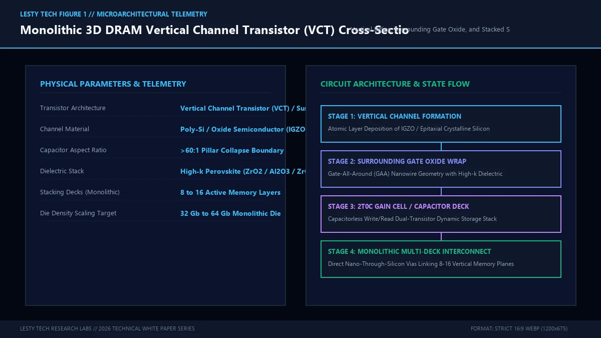
To break through the planar 10nm scaling barrier, the first major architectural revolution is the Vertical Channel Transistor (VCT).
In conventional planar or saddle-fin (FinFET-based) DRAM, the transistor channel lies horizontally along the silicon surface, consuming valuable lateral area between the bitline contact and the capacitor storage node contact. The minimum theoretical cell footprint of a planar folded-bitline layout is constrained to \(6 F^2\), and even aggressive open-bitline layouts cannot scale below \(4 F^2\).
The Vertical Channel Transistor completely upends this geometry by rotating the transistor channel 90 degrees, orienting it vertically perpendicular to the wafer substrate:
- Channel Orientation: The source, channel, and drain are stacked vertically inside a cylindrical silicon or semiconductor pillar. Current flows vertically from the buried bitline at the bottom of the pillar up to the capacitor landing pad at the top.
- Surrounding Gate Architecture (Gate-All-Around GAA): The control wordline wraps completely around the perimeter of the vertical channel cylinder in a true 360-degree Gate-All-Around (GAA) configuration. This delivers maximum electrostatic gate control, eliminating parasitic drain-induced barrier lowering (DIBL) and suppressing short-channel effects even when channel length (\(L_{\text{g}}\)) is scaled down to 15 nanometers.
- Footprint Collapse to \(4 F^2\): Because the transistor channel occupies zero horizontal wafer area, the cell footprint is governed strictly by the intersection of the buried bitline pitch and the vertical wordline pitch, achieving a true \(4.0 F^2\) standard cell area—an immediate 33% silicon area reduction over standard \(6 F^2\) planar cells!
By routing bitlines beneath the transistors as buried metallic lines (using low-resistivity molybdenum or ruthenium), VCT eliminates bitline-to-capacitor parasitic capacitive coupling (\(C_{\text{BL-SN}}\)), slashing signal noise during bitline sensing and expanding sensing voltage margins (\(\Delta V_{\text{sense}} = V_{\text{DD}} / 2 \cdot [C_{\text{cell}} / (C_{\text{cell}} + C_{\text{BL}})]\)).
3. The Capacitorless Revolution: 2T0C Gain Cells & Oxide Semiconductors (IGZO)
While Vertical Channel Transistors solve the lateral footprint problem of the access transistor, they do not eliminate the high-aspect-ratio capacitor pillar. As long as DRAM relies on a physical capacitor to store charge, vertical etching and aspect ratio limits will re-emerge at the 3D level.
To eliminate the capacitor entirely, memory researchers are developing the 2T0C (Two-Transistor, Zero-Capacitor) Gain Cell.
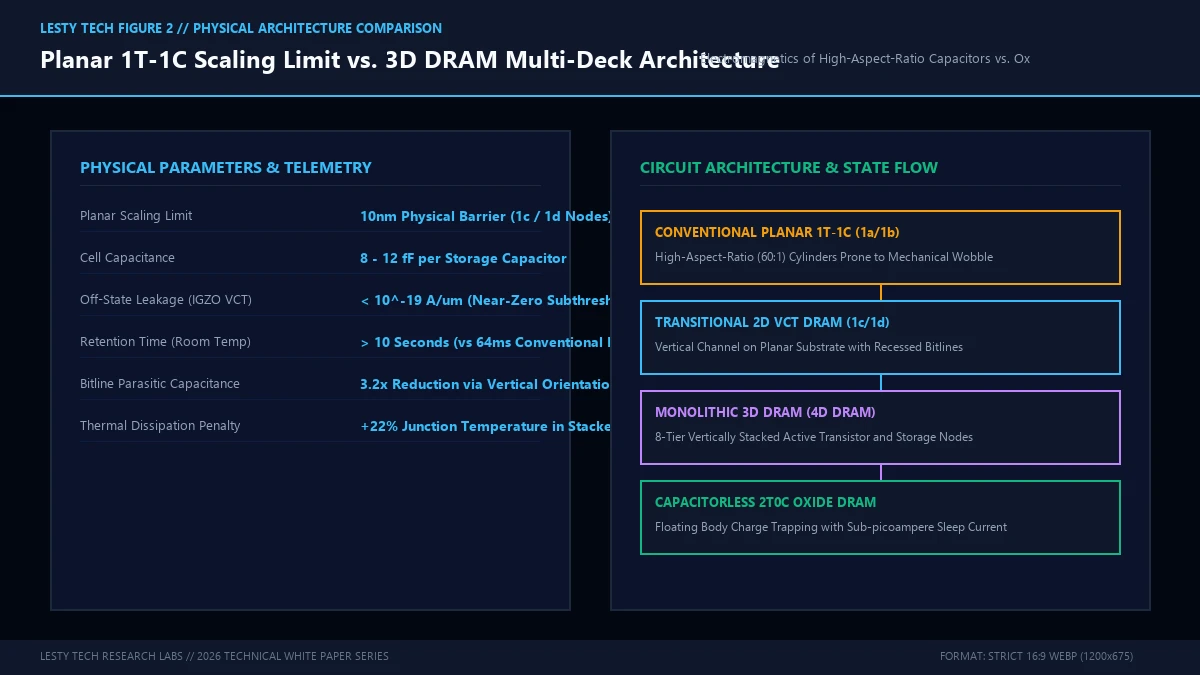
In a 2T0C cell, the physical storage capacitor is completely discarded. Instead, data charge is stored directly on the parasitic gate capacitance of an internal Read Transistor (\(T_{\text{read}}\)), controlled by an adjacent Write Transistor (\(T_{\text{write}}\)):
$$\text{Bit State ‘1’} \implies Q_{\text{stored}} = C_{\text{gate,read}} \cdot V_{\text{write}}$$
When the cell is read, the stored charge modulates the threshold voltage and channel conductance of the Read Transistor, allowing a read current to flow without discharging the stored node! Because the read operation is non-destructive, the cell does not require the immediate post-read precharge restore cycles mandatory in conventional 1T-1C DRAM.
The Breakthrough of Amorphous Oxide Semiconductors (IGZO)
The historical Achilles’ heel of 2T0C capacitorless DRAM was charge leakage. If the write transistor is fabricated from crystalline silicon, its intrinsic sub-threshold off-state leakage current (\(I_{\text{off}} \approx 10^{-14} \text{ to } 10^{-15} \text{ A/\mu m}\)) rapidly drains the tiny gate capacitance within milliseconds, requiring continuous power-hungry refresh operations.
The solution arrived through wide-bandgap Indium Gallium Zinc Oxide (a-IGZO):
| Semiconductor Parameter | Conventional Silicon (Poly-Si) | Amorphous Oxide Semiconductor (IGZO) | Impact on 3D DRAM Physics |
|---|---|---|---|
| Electronic Bandgap (\(E_g\)) | 1.12 eV | 3.1 to 3.4 eV (Wide Bandgap) | Virtually eliminates thermal band-to-band carrier generation |
| Off-State Leakage Current (\(I_{\text{off}}\)) | \(\sim 10^{-14} \text{ A/\mu m}\) | \(< 10^{-19} \text{ A/\mu m}\) (Record Low) | Extends data retention from milliseconds to over 10 seconds! |
| Thermal Deposition Budget | > 800°C (Crystallization Anneal) | < 350°C (BEOL Compatible) | Allows stacking multiple decks directly atop CMOS logic dies |
| Electron Mobility (\(\mu_e\)) | 100 – 300 \(\text{cm}^2/\text{V}\cdot\text{s}\) | 15 – 45 \(\text{cm}^2/\text{V}\cdot\text{s}\) | Sufficient for write drive current while eliminating subthreshold leak |
Because IGZO possesses an extraordinarily wide electronic bandgap (\(E_g \approx 3.2 \text{ eV}\)), its off-state leakage current drops below \(10^{-19} \text{ A/\mu m}\)—nearly five orders of magnitude lower than silicon! A 2T0C IGZO memory cell can store charge on a tiny sub-femtofarad gate node for tens of seconds at room temperature without needing a single refresh command. This slashes DRAM standby refresh power consumption by more than 95%, fundamentally transforming the thermal efficiency of mobile devices and AI accelerator memory.
4. Ferroelectric FET (FeFET / FeRAM) Cells: Polarization Switching Physics
An alternative revolutionary pathway gaining rapid traction across memory research laboratories is the integration of Ferroelectric Gate Dielectrics into 3D DRAM architectures, merging the non-volatility of FeRAM with the sub-nanosecond access speeds of dynamic memory.
Traditional ferroelectric memories utilized perovskite materials like Lead Zirconate Titanate (\(\text{Pb}[\text{Zr}_x\text{Ti}_{1-x}]\text{O}_3\) or PZT). However, PZT suffers from high deposition temperatures, severe lead contamination hazards in silicon cleanrooms, and inability to scale below 50nm film thicknesses. The modern ferroelectric revolution was ignited by the discovery of robust ferroelectricity in doped Hafnium Oxide (\(\text{HfO}_2\))—specifically Hafnium Zirconium Oxide (\(\text{Hf}_{1-x}\text{Zr}_x\text{O}_2\), HZO):
$$P_{\text{net}} = \pm P_r \quad (\text{Remanent Polarization})$$
When an electric field exceeding the coercive field (\(E_c \approx 1.0 \text{ to } 1.5 \text{ MV/cm}\)) is applied across an atomic-layer-deposited HZO film, oxygen atoms within the non-centrosymmetric orthorhombic crystal phase (\(Pca2_1\)) displace microscopically. This ionic displacement generates a permanent, non-volatile dipole polarization (\(P_r \approx 15 \text{ to } 30 \ \mu\text{C/cm}^2\)).
In a Ferroelectric Field-Effect Transistor (FeFET), this remanent polarization directly modulates the channel surface potential of the vertical transistor, producing a wide memory window (\(\text{MW}\)) defined by the threshold voltage separation:
$$\Delta V_{\text{th}} = \text{MW} = 2 \cdot \frac{P_r \cdot t_{\text{fe}}}{\epsilon_{\text{fe}}}$$
Where \(t_{\text{fe}}\) is the ferroelectric film thickness (\(\sim 5 \text{ to } 10 \text{ nm}\)) and \(\epsilon_{\text{fe}}\) is the dielectric permittivity. A positive polarization lowers \(V_{\text{th}}\) (State ‘1’), while a negative polarization elevates \(V_{\text{th}}\) (State ‘0’). Crucially, the read operation simply measures whether current flows at an intermediate gate read voltage (\(V_{\text{read}}\)) without reversing the dipoles. This non-destructive read eliminates DRAM precharge restore cycles and enables near-infinite endurance (> \(10^{12}\) cycles) when paired with engineered inter-layer dielectric barrier interfaces.
5. Monolithic Multi-Deck 3D Stacking: Following 3D NAND into the Third Dimension
Just as NAND flash memory escaped its planar scaling limits in 2013 by transitioning to 3D V-NAND (vertically etching through hundreds of stacked oxide-nitride layers), DRAM is executing a parallel evolution into true Monolithic 3D Stacking (4D DRAM).
Rather than relying on through-silicon vias (TSVs) to bond separate, thick silicon dies (as in 2.5D HBM packaging), Monolithic 3D DRAM fabricates multiple active memory decks sequentially on a single silicon substrate within a single semiconductor manufacturing flow:
- CMOS Under Array (CuA / Periphery-Under-Cell): The noisy, high-voltage peripheral circuitry—including sense amplifiers, row decoders, charge pumps, and column select lines—is fabricated first on the base bulk silicon substrate using standard high-speed CMOS logic processes.
- Inter-Layer Dielectric & Backside Metallization: The logic layer is planarized and covered with an insulating dielectric barrier. Buried vertical power and signal vias are etched to connect periphery drivers to the memory tiers above.
- Sequential Multi-Deck Stacking: Alternating thin films of channel material (poly-Si or IGZO), gate oxide, and wordline metallization are deposited layer-by-layer. Foundries etch continuous vertical holes through all decks simultaneously, depositing the vertical channel pillars in a single high-aspect-ratio lithographic sequence.
By stacking 8, 16, or even 32 memory tiers vertically above a single logic footprint, Monolithic 3D DRAM achieves an astounding density breakthrough. A single 3D DRAM die fabricated on an advanced node will achieve capacities of 32 Gb to 64 Gb per die—more than triple the physical density of the densest planar DRAM dies in existence today!
6. Monolithic Interconnects: Ruthenium Buried Wordlines & Nano-TSV Metrology
As memory decks stack into multi-tier towers, the electrical resistance of wordlines and bitlines presents an existential signal integrity threat. In conventional copper (Cu) metallization, scaling interconnect line widths below 15 nanometers triggers catastrophic resistivity escalation:
$$\rho_{\text{eff}} = \rho_0 \left[ 1 + \frac{3}{8} (1 – p) \frac{\lambda_{\text{bulk}}}{w} + \frac{3}{2} \left( \frac{R}{1 – R} \right) \frac{\lambda_{\text{bulk}}}{d} \right]$$
Where \(\lambda_{\text{bulk}}\) is the electron mean free path (\(\approx 39 \text{ nm}\) in copper), \(p\) is the surface specularity parameter, and \(R\) is the grain boundary reflection coefficient. At sub-15nm dimensions, diffuse electron boundary scattering causes copper resistivity to skyrocket by more than 10x, accompanied by fatal electromigration under high write current densities.
To overcome this interconnect bottleneck, 3D DRAM architectures replace copper on critical buried lines with Ruthenium (Ru) and Molybdenum (Mo). Ruthenium possesses an ultra-short electron mean free path (\(\lambda_{\text{Ru}} \approx 6.6 \text{ nm}\)). At linewidths below 12 nanometers, ruthenium exhibits significantly lower effective resistivity than copper while requiring zero high-resistance diffusion barrier liners (such as TaN/Ta), ensuring pristine signal propagation across thousands of stacked memory nodes.
7. Thermal Dissipation Bottlenecks & Mechanical Stress in 3D Silicon
While Monolithic 3D DRAM resolves the density crisis, it introduces severe thermodynamic and mechanical stress challenges that push materials science to its outer limits.
A. Thermal Resistance in Multi-Tier Stacks
In conventional planar DRAM, all active transistors sit directly on bulk silicon (\(\kappa_{\text{Si}} \approx 148 \text{ W/m}\cdot\text{K}\)), conducting heat efficiently downward toward the package substrate. In Monolithic 3D DRAM, however, active memory decks are interleaved with low-k dielectric isolation layers (\(\text{SiO}_2\) and \(\text{SiOC}\)) possessing miserable thermal conductivities (\(\kappa_{\text{ILD}} \approx 1.2 \text{ to } 1.4 \text{ W/m}\cdot\text{K}\)):
$$R_{\text{thermal, total}} = \sum_{k=1}^{N_{\text{decks}}} \left( \frac{t_{\text{deck}, k}}{\kappa_{\text{metal}} A} + \frac{t_{\text{ILD}, k}}{\kappa_{\text{ILD}} A} \right)$$
Heat generated by continuous high-speed row activations and sense amplifier switching in upper memory decks is physically insulated by multiple underlying oxide layers. Finite-element electro-thermal modeling reveals that an 8-deck 3D DRAM operating under heavy AI inference workloads experiences localized junction temperature increases of 20°C to 35°C above ambient, risking thermal runaway and accelerating subthreshold charge leakage.
B. Mechanical Film Stress & Wafer Bowing
Depositing 16 to 32 alternating layers of metals, high-k dielectrics, and semiconductor channels induces immense cumulative mechanical film stress. Residual tensile and compressive stresses across disparate material interfaces cause severe wafer curvature (wafer bow exceeding \(150 \ \mu\text{m}\)). Excessive wafer bowing leads to extreme lithographic overlay misalignment during deep vertical via etching, requiring stress-compensating backside dielectric capping layers to mechanically balance the wafer during fabrication.
8. Comprehensive Industrial Roadmap: Samsung, SK Hynix, and Micron
The transition to 3D DRAM represents a multi-billion-dollar race among the big three memory titans:
- Samsung Electronics: Samsung formally revealed its 3D DRAM commercial roadmap, confirming the development of sub-10nm Vertical Channel Transistors (VCT) for its transitional nodes, followed by true monolithic multi-deck 3D DRAM targeting production commercialization by 2028-2029. Samsung projects that 3D DRAM will drive single-die densities beyond 100 gigabits.
- SK Hynix: SK Hynix is pioneering amorphous oxide semiconductor (IGZO) integration for capacitorless 2T0C architectures, demonstrating operational prototypes exhibiting retention times exceeding 5 seconds at 85°C. Their roadmap anticipates multi-tier 3D DRAM entering high-volume manufacturing to support next-generation HBM5 and mobile LPDDR6 stacks.
- Micron Technology: Micron has secured dozens of foundational patents covering vertical surround-gate DRAM memory cells and periphery-under-array 3D architectures, focusing on chemical-mechanical planarization (CMP) uniformity and low-temperature atomic layer deposition for sub-10nm memory decks.
3D DRAM vs. 2D Capacitor Limits: Vertical Channel Transistors
Oxide Semiconductors (IGZO), 2T0C Gain Cells, and Monolithic Memory Decks (Complete architectural audit with telemetry tables and schematic breakdowns).
whitepaper_batch_21_1_3d_dram.pdf Format: Publication-Grade PDF
Explore Advanced Semiconductor & Microarchitecture Analyses
Expand your architectural mastery of next-generation solid-state physics, advanced interconnects, and non-volatile materials with these engineering investigations:
- CFET 3D Transistor Stacking vs. GAAFET: Monolithic Silicon Physics & Sub-1nm CMOS
- HBM4 High-Bandwidth Memory: 2048-Bit Logic Base Die & Advanced Interconnect Physics
- Bismuth Antimonide Spintronics: Topological Insulators for Ultra-Low Power MRAM
- Semiconductor Industry Association (SIA): International Technology Roadmap for Semiconductors (External Reference)
In summary, the transition from planar 1T-1C memory to Monolithic 3D DRAM represents the most profound paradigm shift in solid-state memory history. By rotating transistors vertically with surrounding Gate-All-Around architectures, eliminating physical storage capacitors via wide-bandgap IGZO 2T0C gain cells, and stacking active tiers into monolithic 3D decks, 3D DRAM conquers the 10nm physics barrier. It ensures that memory capacity, bandwidth, and energy efficiency will scale dynamically to fuel the computing demands of the coming artificial intelligence century.






No Responses