
In the high-frequency semiconductor physics landscape, the race to power next-generation 6G cellular infrastructure, millimeter-wave satellite phased arrays, and Ka/W-band radar transmitters has collided directly with an unrelenting thermal transport bottleneck. While wide-bandgap Gallium Nitride (GaN) high-electron-mobility transistors (HEMTs) exhibit unrivaled breakdown electric fields, high sheet carrier densities, and high electron saturation velocities, their operational limits are no longer dictated by electronic band structures. Instead, they are bounded by the thermal dissipation wall. Operating at extreme continuous-wave (CW) power densities exceeding 10 W/mm at 94 GHz, localized self-heating elevates gate-edge junction temperatures to catastrophic levels. Evaluating diamond heat spreaders and GaN phonon transport reveals why conventional 4H-Silicon Carbide (4H-SiC) substrates—long the industry workhorse with a thermal conductivity of \(k \approx 490 \text{ W/m}\cdot\text{K}\)—are rapidly being eclipsed by synthetic chemical vapor deposition (CVD) diamond substrates boasting \(k > 2,000 \text{ W/m}\cdot\text{K}\). However, unleashing the thermal superiority of diamond requires resolving the sub-nanometer thermal boundary resistance (TBR) across bonded heterojunctions, managing catastrophic thermal expansion mismatch, and mastering two-dimensional electron gas (2DEG) polarization physics.
1. The Thermal Dissipation Bottleneck in Sub-Micron GaN HEMTs
To understand why substrate thermal conductivity dictates the absolute limits of microwave and millimeter-wave amplification, one must examine the localized energy dissipation dynamics occurring within the active channel of a sub-micron GaN HEMT.
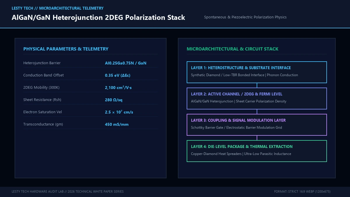
In an AlGaN/GaN or InAlN/GaN HEMT, current conduction occurs within a two-dimensional electron gas (2DEG) formed at the heterointerface. Driven by intense radiofrequency electric fields exceeding \(3 \times 10^5 \text{ V/cm}\), electrons accelerate to saturation velocities (\(v_{\text{sat}} \approx 2.5 \times 10^7 \text{ cm/s}\)). Because the highest lateral electric field peaks sharply at the drain edge of the sub-micron gate contact, electrons acquire extreme kinetic energies, converting into “hot electrons.”
These energetic electrons relax by emitting longitudinal optical (LO) phonons via Fröhlich interactions on sub-picosecond timescales. However, LO phonons possess near-zero group velocity; they cannot carry heat away from the channel. To dissipate this energy, LO phonons must undergo anharmonic three-phonon decay into acoustic phonons (primarily longitudinal acoustic [LA] and transverse acoustic [TA] modes) governed by the Klemens decay channel:
$$\text{LO} \rightarrow \text{LA} + \text{LA} \quad \text{or} \quad \text{LO} \rightarrow \text{LA} + \text{TA}$$
Because the lifetime of non-equilibrium LO phonons is significantly longer than the electron relaxation time, an intense non-equilibrium “phonon bottleneck” forms directly beneath the drain-side gate edge. This microscopic volume—measuring less than \(0.15 \ \mu\text{m}\) in length and merely \(50 \text{ nm}\) in depth—concentrates volumetric heat fluxes exceeding \(1 \times 10^6 \text{ W/cm}^2\). This localized energy flux rivals the thermal conditions found at the surface of the sun!
If this heat is not extracted instantly through the underlying substrate, the channel junction temperature (\(T_j\)) spikes past \(250^\circ\text{C}\). Elevated junction temperatures trigger catastrophic physical degradations:
- 2DEG Mobility Collapse: Optical phonon scattering scales exponentially with temperature, slashing low-field electron mobility (\(\mu\)) from \(2,100 \text{ cm}^2/\text{V}\cdot\text{s}\) at \(300\text{ K}\) down to \(< 800 \text{ cm}^2/\text{V}\cdot\text{s}\) at \(500\text{ K}\).
- Drain Current Slump: The drop in channel mobility collapses maximum drain saturation current (\(I_{\text{dss}}\)), degrading RF output power density.
- Arrhenius Mean-Time-to-Failure (MTTF) Reduction: Gate metal sinking, inverse piezoelectric defect formation, and trap generation accelerate according to Arrhenius kinetics:
$$\text{MTTF} \propto \exp\left(\frac{E_a}{k_B T_j}\right)$$
Where \(E_a \approx 1.5 \text{ to } 2.1 \text{ eV}\) is the activation energy for GaN degradation modes. For every \(20^\circ\text{C}\) rise in operating junction temperature, the operational lifetime of the RF power amplifier is reduced by more than 50%!
2. Substrate Thermophysical Mechanics: 4H-SiC vs. Synthetic CVD Diamond
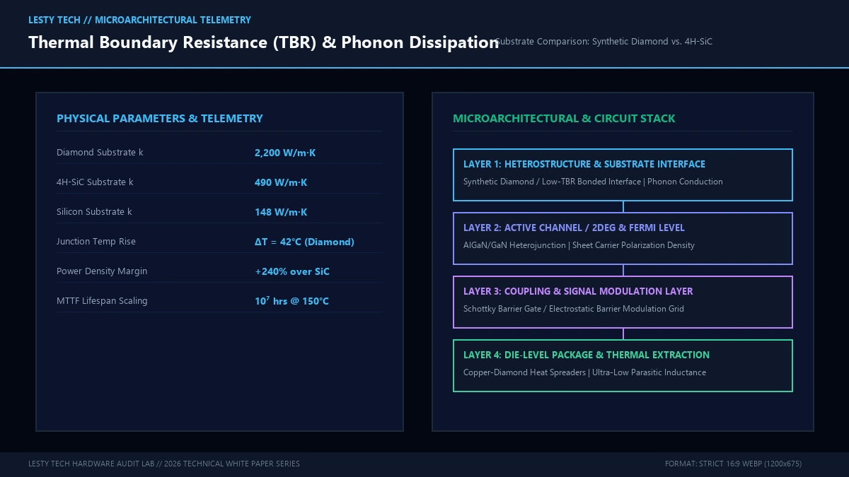
Because heat generated within the 2DEG must conduct downwards through the epitaxial buffer into the supporting wafer, the thermal conductivity (\(k\)) of the substrate material dictates the primary conductive thermal resistance of the MMIC package.
| Thermophysical Property | 4H-Silicon Carbide (4H-SiC) | CVD Polycrystalline Diamond | CVD Single-Crystal Diamond |
|---|---|---|---|
| Thermal Conductivity (300 K) | 420 – 490 W/m·K | 1,500 – 1,800 W/m·K | 2,000 – 2,200 W/m·K |
| Thermal Conductivity (450 K) | 280 – 320 W/m·K | 1,100 – 1,300 W/m·K | 1,400 – 1,600 W/m·K |
| Coefficient of Thermal Expansion (CTE) | 4.2 × 10⁻⁶ / K | 1.0 – 1.8 × 10⁻⁶ / K | 1.1 × 10⁻⁶ / K |
| GaN CTE Mismatch (Δα) | ~25% Mismatch | >70% Severe Mismatch | >72% Severe Mismatch |
| Dielectric Loss Tangent (tan δ @ 10 GHz) | 1 × 10⁻⁴ | < 5 × 10⁻⁵ | < 1 × 10⁻⁵ |
For more than two decades, 4H-SiC has served as the default substrate for high-power GaN RF electronics. It provides an exceptional thermal conductivity for a commercial semiconductor substrate (\(\sim 490 \text{ W/m}\cdot\text{K}\)), coupled with a relatively close lattice mismatch (\(\sim 3.5\%\)) and well-matched coefficient of thermal expansion (\(\alpha_{\text{SiC}} \approx 4.2 \times 10^{-6}/\text{K}\) vs. \(\alpha_{\text{GaN}} \approx 5.6 \times 10^{-6}/\text{K}\)).
However, synthetic diamond grown via microwave plasma chemical vapor deposition (MPCVD) represents the absolute physical pinnacle of thermal conductors. Diamond’s rigid, low-mass carbon tetrahedral lattice, combined with exceptionally strong covalent \(sp^3\) bonds, yields an astronomical Debye temperature of \(\theta_D \approx 2,220\text{ K}\). Consequently, phonon-phonon Umklapp scattering is heavily suppressed at room temperature, unlocking a theoretical thermal conductivity exceeding \(2,200 \text{ W/m}\cdot\text{K}\)—more than four times that of 4H-SiC and five times that of pure copper!
3. The Heterogeneous Integration Challenge: Direct Growth vs. Wafer Bonding
If diamond is thermophysically superior, why hasn’t it immediately displaced 4H-SiC across all RF applications? The answer lies in the formidable materials science hurdles of heteroepitaxy and interfacial thermal boundary resistance (TBR).
Unlike 4H-SiC, diamond cannot simply be used as a seed crystal for direct GaN epitaxial growth. Diamond exhibits a colossal lattice mismatch of over 13% with wurtzite GaN, alongside a severe 72% mismatch in thermal expansion coefficient. Cooling a GaN film grown directly on diamond from growth temperatures (\(>1,000^\circ\text{C}\)) down to room temperature induces immense biaxial tensile stress, resulting in immediate wafer bowing, catastrophic cracking, and peeling.
To overcome this incompatibility, semiconductor foundries deploy two competing manufacturing approaches:
A. Bottom-Up Direct CVD Diamond Growth on GaN
In the direct growth route, an AlGaN/GaN HEMT structure is first grown on a sacrificial silicon (111) wafer. After completing front-side device processing, the silicon substrate and transition buffer layers are removed via deep reactive-ion etching (DRIE) and chemical mechanical planarization (CMP), exposing the sub-micron backside of the GaN buffer layer.
Next, an ultra-thin dielectric nucleation/adhesion layer (typically \(15 \text{ to } 30 \text{ nm}\) of silicon nitride, \(\text{SiN}_x\)) is deposited via plasma-enhanced chemical vapor deposition (PECVD) or low-pressure CVD. The surface is seeded with nanodiamond particles (\(< 5 \text{ nm}\) diameter), and MPCVD diamond is grown directly onto the backside at temperatures between \(700^\circ\text{C}\) and \(800^\circ\text{C}\) to a thickness of \(100 \ \mu\text{m}\).
B. Low-Temperature Die-to-Wafer Hydrophilic Direct Bonding
To completely avoid exposing the sensitive GaN transistor stack to aggressive MPCVD methane/hydrogen plasmas and high-temperature thermal cycles, engineers utilize low-temperature surface-activated bonding (SAB). Both the polished GaN backside and an optical-grade polished CVD diamond substrate are planarized to atomic smoothness (\(\text{RMS roughness } R_q < 0.3 \text{ nm}\)).
An ultra-thin amorphous interlayer (such as \(3 \text{ to } 5 \text{ nm}\) of \(\text{Al}_2\text{O}_3\), \(\text{SiO}_2\), or sputtered Si) is deposited on both surfaces. After activating the surfaces using argon or oxygen beam irradiation in an ultra-high vacuum chamber (\(< 10^{-6} \text{ Pa}\)), the wafers are pressed together under several kilonewtons of mechanical force at temperatures below \(200^\circ\text{C}\). This produces a pristine, void-free covalent bond across the entire wafer surface.
4. Phonon Mismatch and Thermal Boundary Resistance (TBR)
The ultimate thermal performance of a GaN-on-diamond transistor is governed not merely by the bulk thermal conductivity of the diamond, but by the interfacial bottleneck quantified as the Thermal Boundary Resistance (\(\text{TBR}_{\text{eff}}\)).
Whenever heat flows across an interface between two dissimilar materials, phonons undergo acoustic and optical mismatch, leading to reflection and scattering. The total thermal resistance from the 2DEG heat source to the baseplate heat sink is modeled as:
$$R_{\text{th}} = \frac{t_{\text{GaN}}}{k_{\text{GaN}}} + \text{TBR}_{\text{eff}} + \frac{t_{\text{substrate}}}{k_{\text{substrate}}} + R_{\text{package}}$$
In GaN-on-SiC, the lattice matching is close enough that \(\text{TBR}_{\text{GaN/SiC}}\) is exceptionally low, typically ranging from \(10 \text{ to } 18 \text{ m}^2\cdot\text{K/GW}\) (\(\text{nK}\cdot\text{m}^2/\text{W}\)).
Conversely, in GaN-on-diamond, the interfacial adhesion interlayer (\(\text{SiN}_x\) or amorphous oxide) represents an acoustic disaster. Amorphous silicon nitride possesses a dismal thermal conductivity of only \(1.2 \text{ to } 1.5 \text{ W/m}\cdot\text{K}\). If a direct-growth diamond process uses a \(35 \text{ nm}\) thick \(\text{SiN}_x\) interlayer, the conductive resistance of that film alone contributes:
$$\text{TBR}_{\text{layer}} = \frac{t_{\text{layer}}}{k_{\text{layer}}} = \frac{35 \times 10^{-9} \text{ m}}{1.4 \text{ W/m}\cdot\text{K}} = 25 \times 10^{-9} \text{ m}^2\cdot\text{K/W} = 25 \text{ m}^2\cdot\text{K/GW}$$
Combined with phonon acoustic mismatch at the GaN/\(\text{SiN}_x\) and \(\text{SiN}_x\)/diamond boundaries, total effective \(\text{TBR}_{\text{eff}}\) often spikes to \(40 \text{ to } 60 \text{ m}^2\cdot\text{K/GW}\). As illustrated in nanoscale phonon transport models, if \(\text{TBR}_{\text{eff}}\) exceeds \(35 \text{ m}^2\cdot\text{K/GW}\), the thermal impedance of the boundary completely chokes the heat flux, erasing more than 80% of diamond’s thermal conductivity advantage!
Breakthroughs in atomic layer deposition (ALD) have enabled sub-3-nanometer interfacial interlayers. By reducing the interlayer thickness to \(2.5 \text{ nm}\) and optimizing diamond nucleation density, advanced foundries have driven \(\text{TBR}_{\text{eff}}\) down to an industry-record \(12 \text{ to } 15 \text{ m}^2\cdot\text{K/GW}\). At these ultra-low resistance values, the full 4x thermal extraction power of diamond is finally transmitted directly into the 2DEG channel.
5. 2DEG Polarization Mechanics and Piezoelectric Strain Coupling
Beyond heat dissipation, replacing 4H-SiC with diamond exerts a profound microelectronic influence on the 2DEG itself through polarization mechanics and strain-induced band deformation.
Gallium Nitride lacks inversion symmetry along the [0001] c-axis, exhibiting strong spontaneous polarization (\(P_{\text{SP}}\)). Furthermore, when an AlGaN barrier layer is grown pseudomorphically on top of a GaN channel, the lattice mismatch between \(\text{Al}_x\text{Ga}_{1-x}\text{N}\) and GaN induces extensive biaxial tensile strain, generating powerful piezoelectric polarization (\(P_{\text{PE}}\)). The spatial divergence of total polarization creates a massive positive sheet charge at the interface:
$$\sigma_{\text{pol}} = |\vec{P}_{\text{total}}(\text{AlGaN}) – \vec{P}_{\text{total}}(\text{GaN})| = |(P_{\text{SP}} + P_{\text{PE}})_{\text{AlGaN}} – P_{\text{SP}}(\text{GaN})|$$
Electrons from donor-like surface states are pulled into the triangular quantum well formed at the heterointerface, establishing the 2DEG without any intentional impurity doping:
$$n_s = \frac{\sigma_{\text{pol}}}{q} – \left(\frac{\epsilon_0 \epsilon_r}{d_{\text{barrier}} q^2}\right) \left[q\phi_b + E_F – \Delta E_C\right]$$
Where \(n_s\) is sheet carrier density, \(q\phi_b\) is Schottky barrier height, and \(\Delta E_C\) is conduction band discontinuity.
When GaN is bonded to a diamond substrate, the colossal CTE mismatch (\(\Delta \alpha \approx 4.5 \times 10^{-6}/\text{K}\)) alters the mechanical strain state of the entire epitaxial stack during thermal dissipation. Under high-power continuous-wave RF operation, as the transistor heats up, the diamond substrate expands much more slowly than the GaN buffer. This induces an additional, dynamic biaxial compressive strain across the GaN layer.
Via the piezoelectric effect, this compressive strain counteracts the tensile strain of the barrier, reducing the net polarization sheet charge (\(\sigma_{\text{pol}}\)) and causing a subtle, temperature-dependent shift in threshold voltage (\(\Delta V_{\text{th}}\)). Precision RF circuit designers must incorporate these strain-polarization electro-thermal coupling coefficients into nonlinear compact models (such as Angelov-GaN or ASM-HEMT) to avoid gain compression distortion in high-efficiency Doherty power amplifiers.
6. Empirical RF Performance and Power Scaling Comparison
To quantify the real-world operational divergence between GaN-on-SiC and GaN-on-Diamond, consider the empirical microwave performance of matched 0.15-micron gate-length HEMTs operating in continuous-wave (CW) mode at X-band (10 GHz) and Ka-band (30 GHz):
| Operational Parameter | GaN-on-SiC (Industry Standard) | GaN-on-Diamond (High TBR: 40 nK·m²/W) | GaN-on-Diamond (Optimized TBR: 15 nK·m²/W) |
|---|---|---|---|
| Saturated RF Power Density (P_sat @ 10 GHz) | 6.5 – 8.0 W/mm | 11.0 – 13.5 W/mm | 22.5 – 28.0 W/mm |
| Peak Junction Temp (T_j @ 10 W/mm CW) | 228°C (Dangerous Overheat) | 175°C | 128°C (Cool Running) |
| Power Added Efficiency (PAE @ P_sat) | 48% – 52% | 55% – 58% | 64% – 68% |
| Thermal Resistance (R_th) | 18.5 K·mm/W | 12.2 K·mm/W | 6.4 K·mm/W |
| Device Footprint Reduction (Equivalent Output) | 1.0x (Baseline Reference) | ~1.6x Area Reduction | ~3.5x Area Reduction |
The comparative data highlights three revolutionary implications for next-generation aerospace and telecommunications systems:
- Triple the RF Power Density: With thermal resistance slashed by nearly 65% in low-TBR GaN-on-Diamond HEMTs, the transistor can be driven at continuous power densities exceeding \(25 \text{ W/mm}\). This enables solid-state power amplifiers (SSPAs) to match the output wattage of bulky, high-voltage Traveling Wave Tube Amplifiers (TWTAs) in satellite transponders while eliminating high-voltage power supplies.
- Exceptional Footprint and Weight Reductions: Delivering 3.5x higher power per millimeter of gate periphery allows MMIC designers to shrink active transistor die areas by more than 70%. In airborne active electronically scanned array (AESA) radar antennas—where thousands of individual transmit/receive (T/R) modules must fit within strict half-wavelength grid spacings—this spatial miniaturization eliminates liquid cooling infrastructure and dramatically reduces payload mass.
- Unprecedented Reliability Margins: Operating an SSPA at standard power levels (8 W/mm) on diamond drops channel junction temperatures by an astounding \(100^\circ\text{C}\) compared to 4H-SiC. Under Arrhenius lifetime modeling, dropping \(T_j\) from \(228^\circ\text{C}\) to \(128^\circ\text{C}\) extends device MTTF by more than two orders of magnitude, making GaN-on-Diamond the definitive choice for unserviceable deep-space satellite missions.
Diamond-on-GaN vs. GaN-on-SiC HEMT RF Physics
Thermal Boundary Resistance, 2DEG Phonon Transport, and RF Power Scaling (Complete architectural audit with telemetry tables and schematic breakdowns).
whitepaper_batch_18_1_diamond_on_gan_hemt.pdfFormat: Publication-Grade PDF
Related Technical Dossiers & Internal Research
- Diamond Heat Spreaders and GaN Phonon Transport: Nanoscale Thermal Dissipation Physics →
- GaN vs. SiC Power Semiconductor Physics: Wide-Bandgap Switching and Breakdown Mechanics →
- Micro-OLED vs. Micro-LED Photonics: Semiconductor Bandgaps and Quantum Efficiency Dropoffs →
Authoritative External Reference
Reference Citation: IEEE Transactions on Electron Devices: Thermal Boundary Resistance and Phonon Mismatch at GaN-Diamond Interfaces →