
In the high-performance computing (HPC) and artificial intelligence server landscape, data transfer demands between GPUs, custom neural accelerators (TPUs, LPUs), and disaggregated memory pools are expanding exponentially. The PCI Special Interest Group (PCI-SIG) ratified the PCIe 7.0 specification, pushing raw interconnect bandwidth to an astonishing 128 GT/s per lane—translating to 512 GB/s of bidirectional throughput across a standard x16 slot. However, doubling the symbol rate from PCIe 6.0 while maintaining four-level pulse amplitude modulation (PAM4) at a Nyquist frequency of 32 GHz pushes copper electrical channels beyond their physical breaking point. Operating over conventional printed circuit board (PCB) traces (such as Megtron-8 or low-loss PTFE substrates), dielectric absorption and copper skin effect attenuation inflict catastrophic insertion losses exceeding 32 dB per meter. As investigated in Co-Packaged Optics (CPO) and optical transceivers and high-speed storage channels in PCIe Gen5 SSD controller saturation, electrical copper reach has collapsed to mere inches. To maintain rack-scale connectivity across AI clusters, PCIe 7.0 marks the historic transition to optical cabled interconnects and Co-Packaged Optics. Evaluating PCIe 7.0 optical architectures exposes the physics of 64 Gbaud PAM4 eye degradation, flit-level forward error correction (FEC), and sub-picosecond electro-optic conversion.
1. The Copper Channel Insertion Loss Wall at 32 GHz Nyquist
To understand why electrical copper traces cannot bridge server-to-server or chassis-to-chassis distances at 128 GT/s, one must analyze electromagnetic wave propagation through copper transmission lines governed by Maxwell’s equations.
PCIe 7.0 transmits data using 4-level Pulse Amplitude Modulation (PAM4). Because PAM4 encodes two logical bits per analog symbol (00, 01, 10, 11), a raw transfer rate of 128 GT/s corresponds to a baud rate of 64 Gbaud. The fundamental Nyquist frequency (\(f_N\)) required to resolve these transitions is calculated as:
$$f_N = \frac{\text{Baud Rate}}{2} = \frac{64 \text{ Gbaud}}{2} = 32 \text{ GHz}$$
When an electromagnetic signal propagates through a microstrip or stripline on a PCB at 32 GHz, it encounters two primary attenuation mechanisms that scale relentlessly with frequency:
- Conductor Skin Effect Attenuation (\(\alpha_c\)): High-frequency alternating currents do not flow uniformly through the bulk copper conductor. Due to self-induced eddy currents, current density concentrates within an ultra-thin peripheral surface layer known as the skin depth (\(\delta\)):
$$\delta = \sqrt{\frac{\rho}{\pi f \mu_r \mu_0}}$$
At \(f = 32 \text{ GHz}\), the skin depth in standard electrodeposited copper (\(\rho \approx 1.68 \times 10^{-8} \ \Omega\cdot\text{m}\)) collapses to a mere 364 nanometers! Because the current is confined to this sub-micron skin layer, effective conductor resistance skyrockets. Furthermore, if the microscopic surface roughness of the copper foil (\(R_q\)) is comparable to or greater than the skin depth (\(R_q \ge 300\text{ nm}\)), electromagnetic path lengths increase drastically, magnifying conductor loss by an additional 40% to 60%.
- Dielectric Loss (\(\alpha_d\)): As the electric field alternates 32 billion times per second, the molecular dipoles of the surrounding dielectric substrate (e.g., glass fiber reinforced resin) constantly rotate, dissipating electromagnetic energy as localized heat:
$$\alpha_d = \frac{\pi f \sqrt{\epsilon_r}}{c} \tan \delta$$
Where \(\epsilon_r\) is the relative dielectric permittivity and \(\tan \delta\) is the loss tangent (dissipation factor) of the PCB laminate. While skin effect loss scales with \(\sqrt{f}\), dielectric absorption scales linearly with frequency (\(f\))!
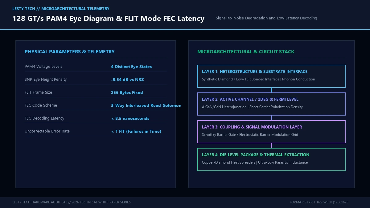
On ultra-premium, low-loss substrates like Megtron-8 (\(\tan \delta \approx 0.0015\)), the combined channel insertion loss at 32 GHz reaches 32 dB per meter (compared to ~14 dB/m at PCIe 5.0’s 16 GHz Nyquist). The standard PCIe 7.0 ball-to-ball channel budget allows a maximum total loss of only 32 dB across the entire channel—including package substrates, ball grid arrays (BGA), PCB traces, via stubs, and connectors.
Subtracting package escape losses (8 dB) and connector discontinuities (4 dB) leaves a usable PCB trace budget of less than 20 dB. In copper, this limits trace reach to less than 9 to 12 inches (22 to 30 cm)! Routing signals from a host CPU to an adjacent chassis, or across an enterprise 19-inch rack backplane, is physically impossible through copper PCB traces without chaining expensive, power-hungry retimer ICs every few inches.
2. PAM4 Signaling Mechanics and the 9.54 dB SNR Penalty
Compounding the severe high-frequency attenuation is the intrinsic signal-to-noise ratio (SNR) degradation imposed by PAM4 modulation.
In legacy Non-Return-to-Zero (NRZ) signaling (utilized in PCIe 1.0 through 5.0), the electrical signal transitions between two voltage levels: High (1) and Low (0). NRZ generates a single, massive eye opening with a vertical eye height of \(V_{\text{ref}}\). In contrast, PAM4 divides the exact same total peak-to-peak voltage envelope (typically 800 mV to 1.0 V) into four distinct signal levels, creating three vertical eye openings stacked atop one another:
| Modulation Level | Bit Pair Mapping | Nominal Voltage (1.0 Vppd) | Relative Amplitude |
|---|---|---|---|
| Level 3 (Top) | 10 |
+500 mV | +1.00 |
| Level 2 (Upper Middle) | 11 |
+167 mV | +0.33 |
| Level 1 (Lower Middle) | 01 |
-167 mV | -0.33 |
| Level 0 (Bottom) | 00 |
-500 mV | -1.00 |
Because each PAM4 eye opening occupies only one-third (\(1/3\)) the vertical amplitude of an NRZ eye, the voltage separation between adjacent decision thresholds collapses to:
$$\Delta V_{\text{PAM4}} = \frac{V_{\text{NRZ}}}{3}$$
Calculating the fundamental Signal-to-Noise Ratio (SNR) degradation in decibels:
$$\text{SNR Loss} = 20 \log_{10}\left(\frac{1}{3}\right) \approx \mathbf{-9.54 \text{ dB}}$$
A 9.54 dB drop means the receiver’s analog front-end (AFE) SerDes must operate in an environment with nearly one-tenth the signal margin of NRZ! Ambient thermal noise, silicon power supply ripple, transmitter phase jitter, and inter-symbol interference (ISI) that would be negligible in NRZ completely collapse the delicate PAM4 eye openings at 64 Gbaud.
3. Flit-Level Forward Error Correction (FEC) and Latency Overhead
Because raw PAM4 channels at 128 GT/s exhibit a First Error Rate (FER) / Bit Error Rate (BER) between \(10^{-4}\) and \(10^{-5}\)—far below PCIe’s mandatory enterprise reliability threshold of \(\text{BER} < 10^{-12}\)—PCIe 7.0 mandates robust Forward Error Correction (FEC).
To eliminate variable packet alignment penalties, PCIe 7.0 operates strictly in Flit (Flow Control Unit) Mode. All transaction layer packets (TLP) and data link layer packets (DLLP) are packetized into fixed-size 256-byte Flits structured as follows:
- 242 Bytes: Protocol Payload Data (TLP and DLLP content).
- 6 Bytes: Cyclic Redundancy Check (CRC-48) for high-integrity error detection.
- 8 Bytes: Reed-Solomon Forward Error Correction parity symbols: \(\text{RS}(256, 248)\) over \(\text{GF}(2^8)\).
The \(\text{RS}(256, 248)\) code can detect and correct up to 4 symbol errors (or a single 8-byte burst error) within each 256-byte Flit. However, computing Reed-Solomon syndrome polynomials, calculating the error locator polynomial via the Berlekamp-Massey algorithm, and finding roots via Chien search introduces serialization and decoding latency.
In ultra-low-latency cache-coherent interconnects (such as CXL 3.1 memory pooling over PCIe 7.0), adding 30 to 50 nanoseconds of FEC decoding delay on every hop would degrade memory load-to-use performance. To prevent this, PCIe 7.0 implements a Lightweight FEC Pipeline with Fast Speculative Commit. The receiver speculatively forwards the incoming payload bytes directly to the upper protocol layers while simultaneously executing syndrome checks in parallel. If no error is detected (which occurs in >99.9% of flits), zero FEC latency is incurred. If a syndrome error is flagged, the pipeline halts, corrects the corrupted symbols, and initiates a local replay via the Link-Level Retry (LLR) state machine.
4. The Optical Interconnect Revolution: CPO and Photonic SerDes
To shatter the 12-inch copper reach limit and connect distributed accelerator clusters across entire datacenters without latency-heavy InfiniBand/Ethernet encapsulation, PCI-SIG established the PCIe Optical Cabled Workgroup.
Rather than converting PCIe packets into Ethernet framing (which incurs TCP/IP or RoCE protocol processing overhead and microsecond-scale latencies), optical PCIe transmits native PCIe Flits directly over fiber-optic waveguides at light speed.
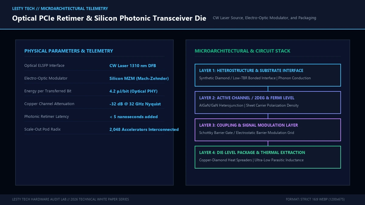
The transition from copper to optics occurs across two evolutionary architectures:
A. Optical PCIe Direct Cables with Active Pluggable Transceivers
In near-term rack-scale deployments, active optical cables (AOC) or pluggable optical modules (OSFP / QSFP-DD) interface directly with server PCIe slots. The electrical SerDes on the motherboard drives a short 4-inch copper trace into a Silicon Photonics (SiPh) engine embedded within the transceiver connector. Inside the module:
- Continuous-Wave (CW) DFB laser diodes supply unmodulated light at 1310 nm (O-band).
- Mach-Zehnder Modulators (MZM) or Micro-Ring Modulators (MRM) convert electrical PAM4 voltages into modulated optical pulses.
- Light travels through multi-mode or single-mode optical fiber with an attenuation of only 0.3 dB per kilometer—virtually zero signal loss across datacenter distances!
B. Co-Packaged Optics (CPO) and Monolithic Photonic Die Integration
The ultimate implementation of PCIe 7.0 bypasses PCB copper traces entirely through Co-Packaged Optics. As analyzed in recent optical networking breakthroughs, CPO places the Silicon Photonics transceiver die directly onto the same organic multi-chip packaging substrate alongside the host GPU or CPU processor.
High-density 2.5D silicon bridges (such as Intel EMIB or TSMC CoWoS) interconnect the GPU compute die with the optical engine over micro-bumps at sub-millimeter distances. Because the electrical trace length is shorter than 5 millimeters, electrical parasitic capacitance and trace attenuation are virtually eradicated:
| Interconnect Technology | Reach Distance @ 128 GT/s | Energy Consumption (pJ/bit) | Channel Latency | Baud Rate / Modulation |
|---|---|---|---|---|
| Standard Copper PCB Trace | < 0.3 meters (< 12 inches) | 18 – 24 pJ/bit (with Retimers) | ~8 – 15 ns (Retimer delays) | 64 Gbaud PAM4 |
| Twinaxial Copper Cable | ~1.0 meter (~3.3 feet) | 14 – 18 pJ/bit | ~5 ns / meter | 64 Gbaud PAM4 |
| Pluggable Optical Transceiver | Up to 100 meters | 10 – 14 pJ/bit | ~4.9 ns / meter (Fiber) | 64 Gbaud PAM4 Optical |
| Co-Packaged Optics (CPO) | Up to 2,000 meters | < 4.5 pJ/bit | < 5 ns Total Channel Delay | Direct Optical Flits |
By eliminating high-power SerDes equalizers and copper retimer chips, CPO slashes interconnect power consumption from 20 pJ/bit down to under 4.5 pJ/bit. For an AI cluster comprising 1,024 GPUs communicating over all-to-all networks, this 75% energy reduction saves hundreds of kilowatts of power purely in interconnect dissipation.
5. Latency and Coherent Memory Fabrics: CXL 3.1 Convergence
The fusion of PCIe 7.0 and optical interconnects yields its most transformative impact in disaggregated, cache-coherent memory fabrics through Compute Express Link (CXL 3.1).
Modern AI foundation models exceed the physical memory capacity of individual GPU nodes. Distributed training requires exchanging activation tensors, gradients, and optimizer states across thousands of accelerators. Historically, this required RDMA over Converged Ethernet (RoCE) or InfiniBand networks, which introduce software network stack overhead, packet serialization delays, and queue contention—pushing memory access latencies into the hundreds of nanoseconds or low microseconds.
Optical PCIe 7.0 running CXL 3.1 protocols enables Direct Optical Load/Store Memory Access:
- True Cache Coherency: CXL.mem and CXL.cache protocols allow an accelerator to issue native 64-byte memory read and write instructions directly into a remote memory pool located in another server chassis across the optical fabric.
- Sub-100-Nanosecond Memory Access: With fiber propagation adding merely 4.9 ns per meter and near-zero protocol overhead in optical CPO SerDes, accessing memory across a 10-meter optical cable completes in less than 85 nanoseconds! This is comparable to the local NUMA memory latency of dual-socket server motherboards.
- Multi-Tier Memory Pooling: Datacenter operators can dynamically pool terabytes of CXL memory and assign it elastically to compute nodes on demand, completely eliminating stranded DRAM across cloud server fleets.
6. Continuous-Time Linear Equalization (CTLE) and DFE in 64 Gbaud Receivers
To grasp why optical links deliver such a decisive power advantage over copper, one must analyze the extreme complexity of electrical receiver equalization required at 64 Gbaud.
When an electrical signal passes through a high-loss PCB trace, the high-frequency components are attenuated far more severely than the DC components, resulting in severe Inter-Symbol Interference (ISI). To reconstruct the collapsed PAM4 eye diagram at the receiver, the analog front-end (AFE) must implement a complex, multistage equalization cascade:
- Continuous-Time Linear Equalization (CTLE): An analog high-pass filter with tunable peaking and zero frequencies that boosts 32 GHz high-frequency gain by 12 to 18 dB relative to low frequencies. However, CTLE inherently amplifies high-frequency channel crosstalk and thermal noise alongside the desired signal.
- Feed-Forward Equalization (FFE): A multi-tap finite impulse response filter (typically 3 to 5 taps) at the transmitter or receiver that shapes precursor and postcursor inter-symbol transitions.
- Decision Feedback Equalization (DFE): A non-linear recursive filter that subtracts the calculated ISI tail of previously decided symbols from the currently sampled symbol.
At 64 Gbaud, the symbol period (\(T_s\)) is an unfathomably short 15.625 picoseconds! In a standard DFE architecture, the first feedback tap (Tap 1) must resolve the slicer decision, compute the feedback voltage, and subtract it from the input node within a single symbol period (\(< 15.6 \text{ ps}\)). Fabricating an analog loop that completes feedback subtraction in 15 picoseconds exceeds the transistor switching speeds of even modern 3nm FinFET / GAAFET silicon nodes!
To bypass this timing impossibility, electrical SerDes designers must resort to “unrolled” or speculative DFE architectures, evaluating all four possible previous PAM4 levels in parallel. This quadruples the number of slicers, clock distribution networks, and power-hungry summing amplifiers. A 128 GT/s electrical copper SerDes consumes between 14 and 18 milliwatts per gigabit/sec, turning receiver silicon into miniature heat radiators.
In contrast, an optical link presents virtually zero high-frequency dispersion over datacenter distances. Because the fiber-optic channel does not exhibit severe high-frequency roll-off, optical SerDes can operate with minimal, low-power CTLE and completely eliminate the power-hungry speculative DFE engine—slashing receiver silicon area and dynamic power dissipation by more than 60%.
7. Thermal and Reliability Engineering in Optical PCIe Enclosures
While optical PCIe 7.0 delivers unprecedented reach and bandwidth density, deploying photonic engines in dense enterprise servers introduces rigorous thermal and reliability engineering challenges.
Continuous-Wave (CW) Distributed Feedback (DFB) laser diodes are highly sensitive to thermal fluctuations. As junction temperatures rise, the optical emission wavelength shifts according to semiconductor bandgap narrowing (\(\Delta \lambda / \Delta T \approx 0.1 \text{ nm/}^\circ\text{C}\)), while optical output power degrades exponentially. Operating an internal laser inside an AI server chassis where GPUs exhaust air at \(65^\circ\text{C}\) to \(75^\circ\text{C}\) causes rapid laser threshold degradation and premature failure.
To ensure 10-year enterprise reliability, the PCIe 7.0 optical specification mandates External Laser Source (ELS) Architectures:
- External Laser Mates (ELM): High-power CW lasers are decoupled from the hot GPU packaging substrate and housed inside dedicated, coolable blind-mate modules mounted on the front panel of the chassis.
- Polarization-Maintaining Fiber (PMF): Unmodulated laser power is fed from the front-panel ELS module to the package-mounted CPO optical engine via polarization-maintaining fiber ribbons.
- Blind-Mate Optical Connectors: Blind-mate expanded-beam optical connectors (such as PRIZM MT or multi-fiber push-on lenses) allow hot-swapping server sleds without manual fiber splicing or risk of microscopic dust contamination destroying optical interfaces.
By decoupling the light source from the thermal dissipation envelope of high-wattage computing silicon, optical PCIe 7.0 achieves telecom-grade reliability (\(\text{MTBF} > 10^7 \text{ hours}\)) while establishing the fundamental physical highway that will drive artificial general intelligence computing architectures into the next decade.
PCIe 7.0 at 128 GT/s: Optical Interconnects & PAM4 Physics
Channel Insertion Loss, Flit-Level FEC, and Dielectric Attenuation (Complete architectural audit with telemetry tables and schematic breakdowns).
whitepaper_batch_18_4_pcie7_optical_interconnects.pdfFormat: Publication-Grade PDF
Related Technical Dossiers & Internal Research
- Co-Packaged Optics (CPO) vs. Pluggable Optical Transceivers: The 51.2T Switch Thermal Limit →
- PCIe Gen5 SSD Thermal Throttling: NAND Flash Controller Saturation →
- Optical Circuit Switches (OCS) in Datacenter Fabrics: Direct MEMS Mirror Beam Steering →
Authoritative External Reference
Reference Citation: PCI-SIG Official Specification: PCIe 7.0 Channel Insertion Loss and Optical Architecture Standards →